MicroBlaze Processor Reference Guide 156
UG984 (v2018.2) June 21, 2018 www.xilinx.com
Chapter 3: MicroBlaze Signal Interface Description
Byte_Enable[0:3]
The byte enable signals are outputs from the core and indicate which byte lanes of the data
bus contain valid data.
Byte_Enable[0:3]is valid only when AS is high. In multicycle
accesses requiring more than one clock cycle to complete),
Byte_Enable[0:3]is valid only
in the first clock cycle of the transfer. Valid values for
Byte_Enable[0:3]are shown in the
following table:
Data_Write[0:31]
The write data bus is an output from the core and contains the data that is written to
memory. It is valid only when AS is high. Only the byte lanes specified by
Byte_Enable[0:3]contain valid data.
AS
The address strobe is an output from the core and indicates the start of a transfer and
qualifies the address bus and the byte enables. It is high only in the first clock cycle of the
transfer, after which it goes low and remains low until the start of the next transfer.
Read_Strobe
The read strobe is an output from the core and indicates that a read transfer is in progress.
This signal goes high in the first clock cycle of the transfer, and can remain high until the
clock cycle after Ready is sampled high. If a new read transfer is directly started in the next
clock cycle, then
Read_Strobe remains high.
Write_Strobe
The write strobe is an output from the core and indicates that a write transfer is in progress.
This signal goes high in the first clock cycle of the transfer, and can remain high until the
clock cycle after Ready is sampled high. If a new write transfer is directly started in the next
clock cycle, then
Write_Strobe remains high.
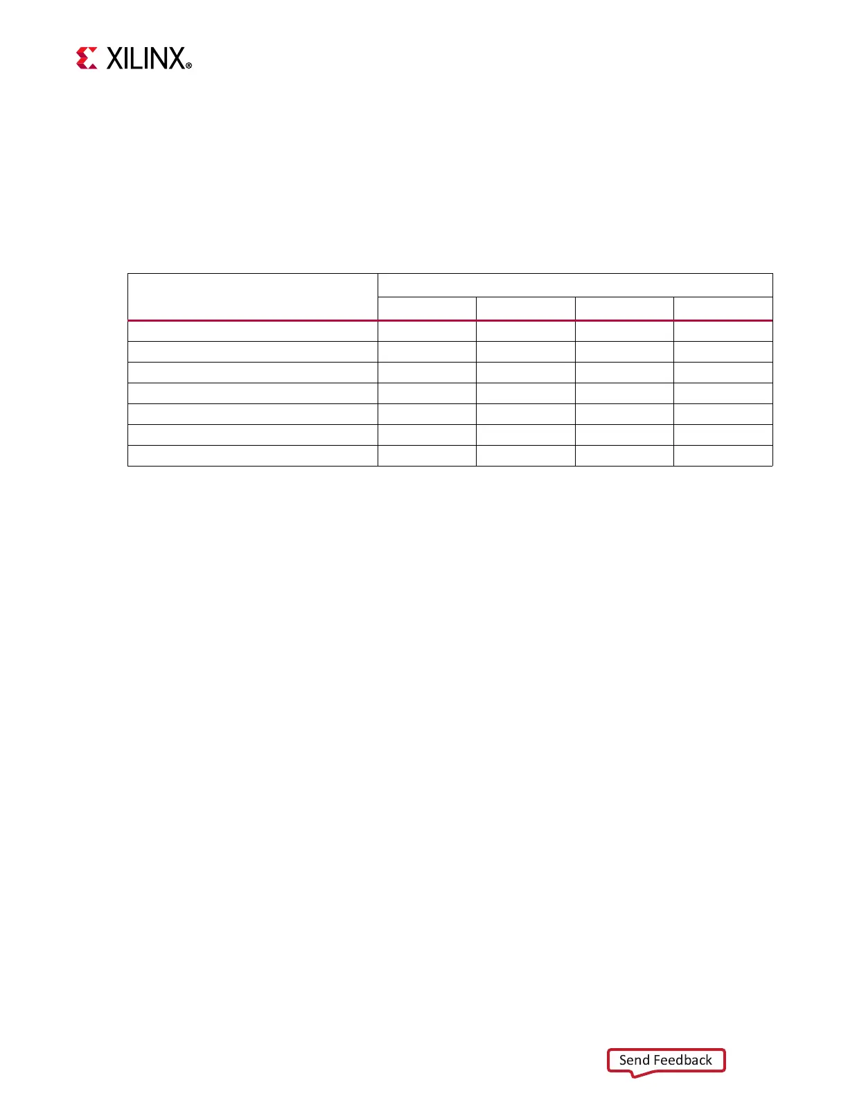
Table 3-8: Valid Values for Byte_Enable[0:3]
Byte_Enable[0:3]
Byte Lanes Used
Data[0:7] Data[8:15] Data[16:23] Data[24:31]
0001 •
0010 •
0100 •
1000 •
0011 ••
1100 ••
1111 ••••