MicroBlaze Processor Reference Guide 86
UG984 (v2018.2) June 21, 2018 www.xilinx.com
Chapter 2: MicroBlaze Architecture
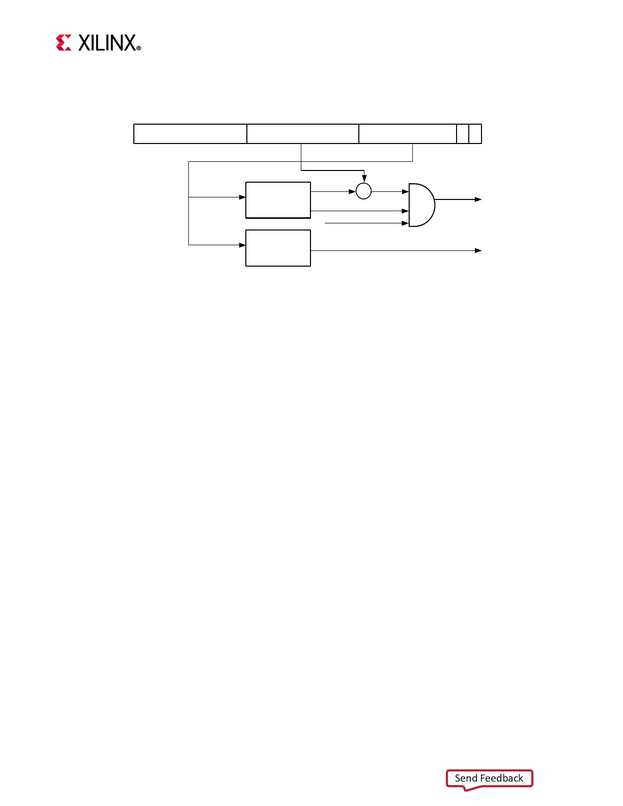
The following figure shows the Data Cache organization.
The cacheable data address consists of two parts: the cache address, and the tag address.
The MicroBlaze data cache can be configured from 64 bytes to 64 kB. This corresponds to
a cache address of between 6 and 16 bits. The tag address together with the cache address
should match the full address of cacheable memory. When selecting cache sizes below 2 kB,
distributed RAM is used to implement the Tag RAM and Data RAM, except that block RAM
is always used for the Data RAM when
C_AREA_OPTIMIZED is set to 1 (Area) and
C_DCACHE_USE_WRITEBACK is not set. Distributed RAM is always used to implement the Tag
RAM, when setting the parameter
C_DCACHE_FORCE_TAG_LUTRAM to 1. This parameter is
only available with cache size 8 kB and less for 4 word cache-lines, with 16 kB and less for
8 word cache-lines, and with 32 kB and less for 16 word cache-lines.
For example, in a MicroBlaze configured with C_DCACHE_BASEADDR=0x00400000,
C_DCACHE_HIGHADDR=0x00403fff, C_DCACHE_BYTE_SIZE=2048, C_DCACHE_LINE_LEN=4,
and
C_DCACHE_FORCE_TAG_LUTRAM=0; the cacheable memory of 16 kB uses 14 bits of byte
address, and the 2 kB cache uses 11 bits of byte address, thus the required address tag
width is 14-11=3 bits. The total number of block RAM primitives required in this
configuration is 1 RAMB16 for storing the 512 data words, and 1 RAMB16 for 128 cache line
entries, each consisting of 3 bits of tag, 4 word-valid bits, 1 line-valid bit. In total, 2 RAMB16
primitives.
Data Cache Operation
The caching policy used by the MicroBlaze data cache, write-back or write-through, is
determined by the parameter
C_DCACHE_USE_WRITEBACK. When this parameter is set, a
write-back protocol is implemented; otherwise write-through is implemented.
However, when configured with an MMU (C_USE_MMU > 1, C_AREA_OPTIMIZED = 0
(Performance) or 2 (Frequency),
C_DCACHE_USE_WRITEBACK = 1), the caching policy in
virtual mode is determined by the W storage attribute in the TLB entry, whereas write-back
is used in real mode.
X-Ref Target - Figure 2-23
Figure 2-23: Data Cache Organization
Tag Address Cache Word Address
Data Address Bits
- -
=
Tag
RAM
Addr
Tag
Valid
Cache_Hit
Data
RAM
Addr
Cache_data
Load_Instruction
0 30 31
X19760-091317