MicroBlaze Processor Reference Guide 136
UG984 (v2018.2) June 21, 2018 www.xilinx.com
Chapter 3: MicroBlaze Signal Interface Description
MicroBlaze I/O Overview
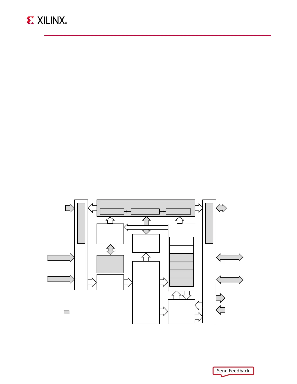
The core interfaces shown in the following figure and Table 3-1 are defined as follows:
• M_AXI_DP: Peripheral Data Interface, AXI4-Lite or AXI4 interface
• DLMB: Data interface, Local Memory Bus (BRAM only)
• M_AXI_IP: Peripheral Instruction interface, AXI4-Lite interface
• ILMB: Instruction interface, Local Memory Bus (BRAM only)
• M0_AXIS..M15_AXIS: AXI4-Stream interface master direct connection interfaces
• S0_AXIS..S15_AXIS: AXI4-Stream interface slave direct connection interfaces
• M_AXI_DC: Data-side cache AXI4 interface
• M_ACE_DC: Data-side cache AXI Coherency Extension (ACE) interface
• M_AXI_IC: Instruction-side cache AXI4 interface
• M_ACE_IC: Instruction-side cache AXI Coherency Extension (ACE) interface
• Core: Miscellaneous signals for: clock, reset, interrupt, debug, trace
X-Ref Target - Figure 3-1
Figure 3-1: MicroBlaze Core Block Diagram
Bus
IF
I-Cache
Instruction
Buffer
Instruction
Buffer
Branch Target
Cache
Program
Counter
M_AXI_IC
Memory Management Unit (MMU)
ITLB DTLBUTLB
Bus
IF
D-Cache
M_AXI_DC
M_AXI_DP
DLMB
M0_AXIS ..
M15_AXIS
S0_AXIS ..
S15_AXIS
Special
Purpose
Registers
Instruction
Decode
Register File
32 x 32b
ALU
Shift
Barrel Shift
Multiplier
Divider
FPU
Instruction-side
Bus interface
Data-side
Bus interface
Optional MicroBlaze feature
M_AXI_IP
ILMB
M_ACE_DC
M_ACE_IC
X19738-091117