MicroBlaze Processor Reference Guide 169
UG984 (v2018.2) June 21, 2018 www.xilinx.com
Chapter 3: MicroBlaze Signal Interface Description
Debug Interface Description
The debug interface on MicroBlaze is designed to work with the Xilinx Microprocessor
Debug Module (MDM) IP core. The MDM is controlled by the Xilinx System Debugger
(XSDB) through the JTAG port of the FPGA. The MDM can control multiple MicroBlaze
processors at the same time. The debug signals are grouped in the DEBUG bus.
The debug interface can be grouped in the DEBUG bus, using either JTAG serial signals (by
setting
C_DEBUG_INTERFACE = 0) or the AXI4-Lite compatible parallel signals (by setting
C_DEBUG_INTERFACE = 1). The MDM configuration must also be set accordingly.
It is also possible to use only AXI4-Lite parallel signals (C_DEBUG_INTERFACE = 2) grouped
in an AXI4 bus, in case the MDM is not used. However, this configuration is not supported
by the tools.
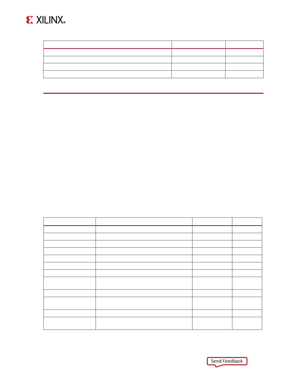
Table 3-15 lists the debug signals on MicroBlaze.
Trace_MEM_PipeRun 3227 std_logic
Trace_MB_Halted 3228 std_logic
Trace_Jump_Hit 3229 std_logic
Reserved 3230 to 4095
1. This signal is only used when C_INTERCONNECT = 3 (ACE).
Table 3-15: MicroBlaze Debug Signals
Signal Name Description VHDL Type Kind
Dbg_Clk JTAG clock from MDM std_logic serial in
Dbg_TDI JTAG TDI from MDM std_logic serial in
Dbg_TDO JTAG TDO to MDM std_logic serial out
Dbg_Reg_En Debug register enable from MDM std_logic_vector serial in
Dbg_Shift
1
JTAG BSCAN shift signal from MDM std_logic serial in
Dbg_Capture JTAG BSCAN capture signal from MDM std_logic serial in
Dbg_Update JTAG BSCAN update signal from MDM std_logic serial in
Debug_Rst
1
Reset signal from MDM, active high. Should
be held for at least 1
Clk clock cycle.
std_logic input
Dbg_Trig_In
2
Cross trigger event input to MDM std_logic_vector output
Dbg_Trig_Ack_In
2
Cross trigger event input acknowledge from
MDM
std_logic_vector input
Dbg_Trig_Out
2
Cross trigger action output from MDM std_logic_vector input
Dbg_Trig_Ack_Out
2
Cross trigger action output acknowledge to
MDM
std_logic_vector output
Table 3-14: MicroBlaze Lockstep Comparison Signals (Cont’d)
Signal Name Bus Index Range VHDL Type