MicroBlaze Processor Reference Guide 170
UG984 (v2018.2) June 21, 2018 www.xilinx.com
Chapter 3: MicroBlaze Signal Interface Description
The parallel debug clock DEBUG_ACLK can usually be connected to the same source as Clk.
However, in case Clk is stopped to save power, the parallel debug clock should be
connected before the clock control buffer (to the Clock input signal in
Figure 3-2 and
Figure 3-3), otherwise debugging is not possible when Clk is stopped.
In most cases, the parallel debug reset DEBUG_ARESET can be directly connected to the
same source as Reset. However, in case software reset is implemented to only reset the
processor, parallel debug reset should not be affected by the software reset, to ensure that
debugging is not disturbed.
Dbg_Trace_Data
3
External Program Trace data output to MDM std_logic_vector output
Dbg_Trace_Valid
3
External Program Trace valid to MDM std_logic output
Dbg_Trace_Ready
3
External Program Trace ready from MDM std_logic input
Dbg_Trace_Clk
3
External Program Trace clock from MDM std_logic input
Dbg_ARADDR
4
Read address from MDM std_logic_vector parallel in
Dbg_ARREADY
4
Read address ready to MDM std_logic parallel out
Dbg_ARVALID
4
Read address valid from MDM std_logic parallel in
Dbg_AWADDR
4
Write address from MDM std_logic_vector parallel in
Dbg_AWREADY
4
Write address ready to MDM std_logic parallel out
Dbg_AWVALID
4
Write address valid from MDM std_logic parallel in
Dbg_BREADY
4
Write response ready to MDM std_logic parallel out
Dbg_BRESP
4
Write response to MDM std_logic_vector parallel out
Dbg_BVALID
4
Write response valid from MDM std_logic parallel in
Dbg_RDATA
4
Read data to MDM std_logic_vector parallel out
Dbg_RREADY
4
Read data ready to MDM std_logic parallel out
Dbg_RRESP
4
Read data response to MDM std_logic_vector parallel out
Dbg_RVALID
4
Read data valid from MDM std_logic parallel in
Dbg_WDATA
4
Write data from MDM std_logic_vector parallel in
Dbg_WREADY
4
Write data ready to MDM std_logic parallel out
Dbg_WVALID
4
Write data valid from MDM std_logic parallel in
DEBUG_ACLK
4
Debug clock, must be synchronous to Clk std_logic parallel in
DEBUG_ARESET
4
Debug reset, must be synchronous to Clk std_logic parallel in
1. Updated for MicroBlaze v7.00: Dbg_Shift added and Debug_Rst included in DEBUG bus
2. Updated for MicroBlaze v9.3: Dbg_Trig signals added to DEBUG bus
3. Updated for MicroBlaze v9.4: External Program Trace signal added to DEBUG bus
4. Updated for MicroBlaze v10.0: Parallel debug signals added to DEBUG bus
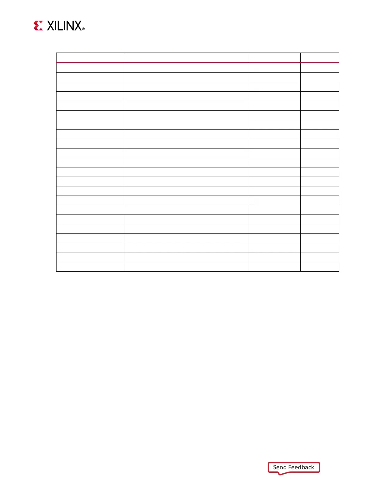
Table 3-15: MicroBlaze Debug Signals (Cont’d)
Signal Name Description VHDL Type Kind