MicroBlaze Processor Reference Guide 26
UG984 (v2018.2) June 21, 2018 www.xilinx.com
Chapter 2: MicroBlaze Architecture
Special Purpose Registers
Program Counter (PC)
The program counter (PC) is the 32-bit address of the execution instruction. It can be read
with an MFS instruction, but it cannot be written with an MTS instruction. When used with
the MFS instruction the PC register is specified by setting Sa = 0x0000. The following figure
illustrates the PC and
Table 2-8 provides a description and reset value.
Machine Status Register (MSR)
The Machine Status Register contains control and status bits for the processor. It can be
read with an MFS instruction. When reading the MSR, bit 29 is replicated in bit 0 as the carry
copy. MSR can be written using either an
MTS instruction or the dedicated MSRSET and
MSRCLR instructions.
When writing to the MSR using MSRSET or MSRCLR, the Carry bit takes effect immediately
and the remaining bits take effect one clock cycle later. When writing using MTS, all bits
take effect one clock cycle later. Any value written to bit 0 is discarded.
When used with an MTS or MFS instruction, the MSR is specified by setting Sx = 0x0001.
The following table illustrates the MSR register and
Table 2-9 provides the bit description
and reset values.
X-Ref Target - Figure 2-3
Figure 2-3: PC
Table 2-8: Program Counter (PC)
Bits Name Description Reset Value
0:31 PC Program Counter
Address of executing instruction, that is, “mfs r2, 0” stores the
address of the mfs instruction itself in R2.
0x00000000
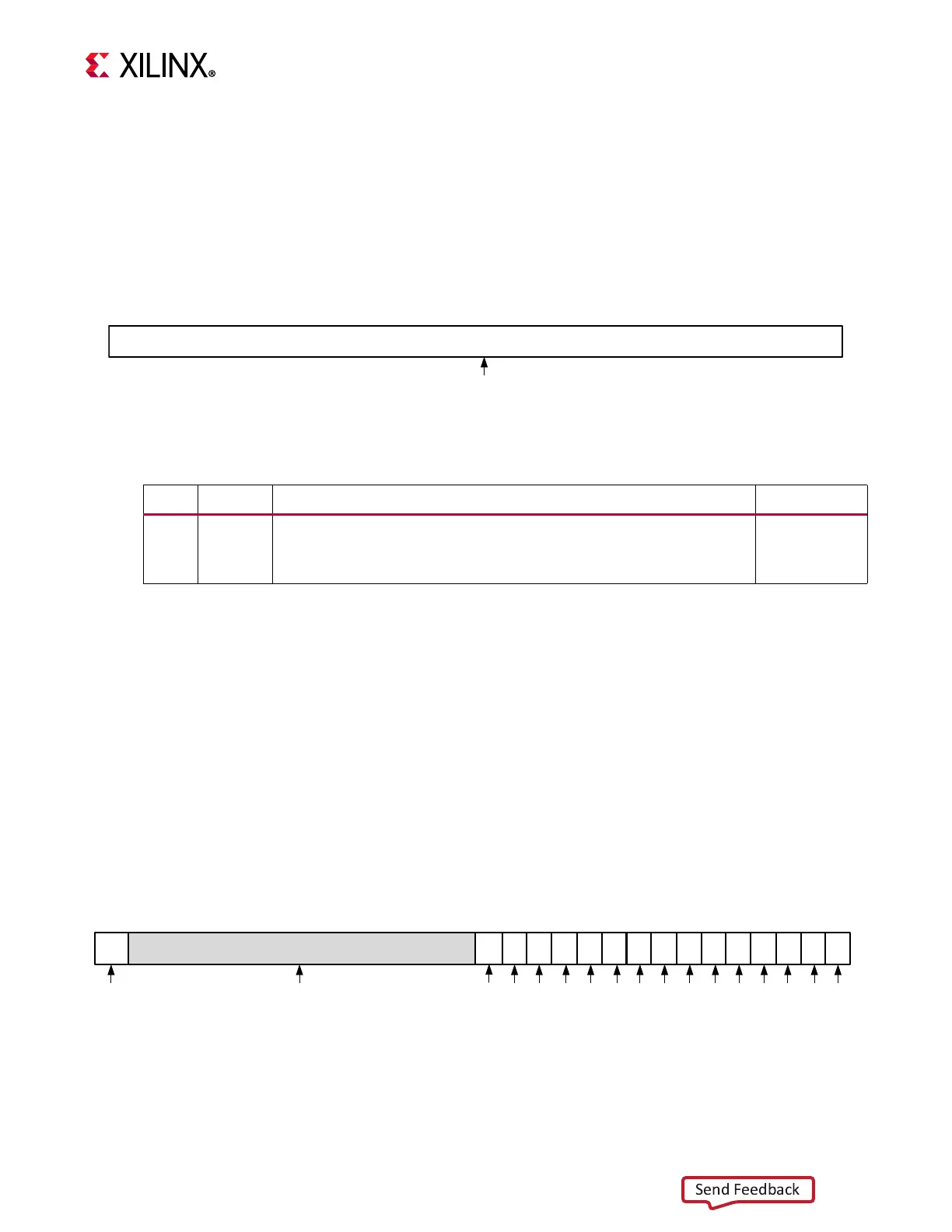
X-Ref Target - Figure 2-4
Figure 2-4: MSR
31
RES
ReservedCC
0
3029282726252423222120191817
IECBIPFSLICEDZODCEEEEIPPVRUMUMSVMVMS
X19741-091117