MicroBlaze Processor Reference Guide 11
UG984 (v2018.2) June 21, 2018 www.xilinx.com
Chapter 2: MicroBlaze Architecture
Data Types and Endianness
The MicroBlaze processor uses Big-Endian or Little-Endian format to represent data,
depending on the selected endianness. The parameter
C_ENDIANNESS is set to 1 (little-
endian) by default.
The hardware supported data types for MicroBlaze are word, half word, and byte. When
using the reversed load and store instructions LHUR, LWR, SHR, and SWR, the bytes in the
data are reversed, as indicated by the byte-reversed order.
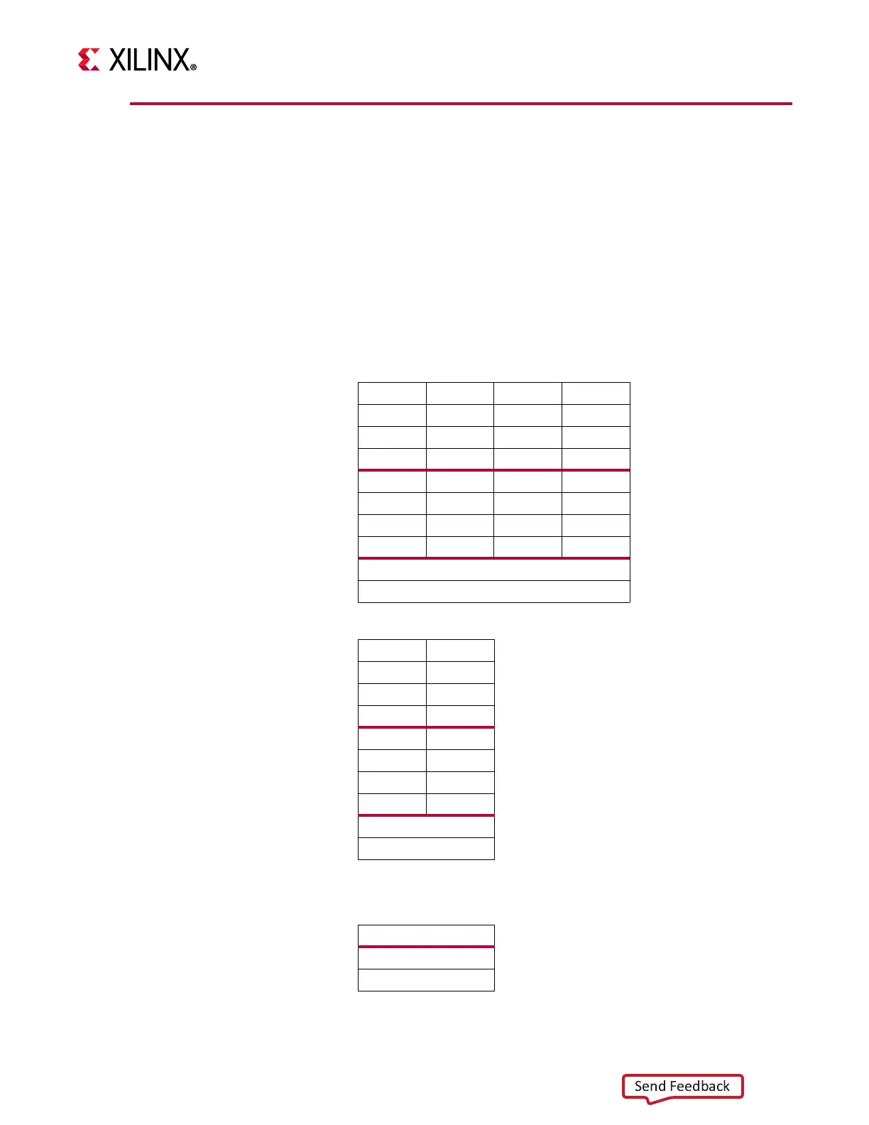
The following tables show the bit and byte organization for each type.
Table 2-2: Word Data Type
Big-Endian Byte Address n n+1 n+2 n+3
Big-Endian Byte Significance MSByte LSByte
Big-Endian Byte Order n n+1 n+2 n+3
Big-Endian Byte-Reversed Order n+3 n+2 n+1 n
Little-Endian Byte Address n+3 n+2 n+1 n
Little-Endian Byte Significance MSByte LSByte
Little-Endian Byte Order n+3 n+2 n+1 n
Little-Endian Byte-Reversed Order n n+1 n+2 n+3
Bit Label 0 31
Bit Significance MSBit LSBit
Table 2-3: Half Word Data Type
Big-Endian Byte Address n n+1
Big-Endian Byte Significance MSByte LSByte
Big-Endian Byte Order n n+1
Big-Endian Byte-Reversed Order n+1 n
Little-Endian Byte Address n+1 n
Little-Endian Byte Significance MSByte LSByte
Little-Endian Byte Order n+1 n
Little-Endian Byte-Reversed Order n n+1
Bit Label 0 15
Bit Significance MSBit LSBit
Table 2-4: Byte Data Type
Byte Address n
Bit Label 0 7
Bit Significance MSBit LSBit