MicroBlaze Processor Reference Guide 7
UG984 (v2018.2) June 21, 2018 www.xilinx.com
Chapter 2
MicroBlaze Architecture
Introduction
This chapter contains an overview of MicroBlaze™ features and detailed information on
MicroBlaze architecture including Big-Endian or Little-Endian bit-reversed format, 32-bit
general purpose registers, virtual-memory management, cache software support, and
AXI4-Stream interfaces.
Overview
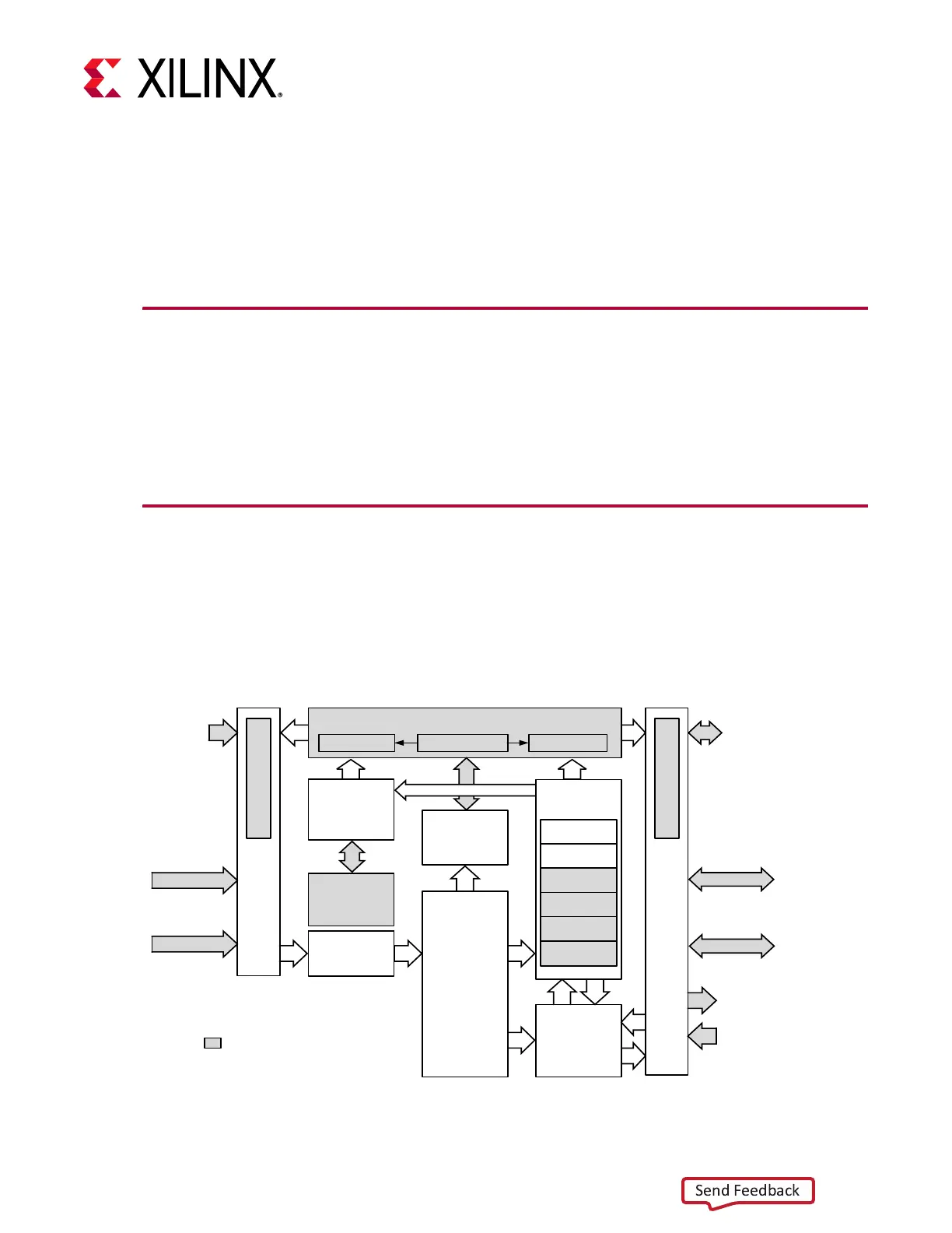
The MicroBlaze embedded processor soft core is a reduced instruction set computer (RISC)
optimized for implementation in Xilinx® Field Programmable Gate Arrays (FPGAs). The
following figure shows a functional block diagram of the MicroBlaze core.
X-Ref Target - Figure 2-1
Figure 2-1: MicroBlaze Core Block Diagram
Bus
IF
I-Cache
Instruction
Buffer
Instruction
Buffer
Branch Target
Cache
Program
Counter
M_AXI_IC
Memory Management Unit (MMU)
ITLB DTLBUTLB
Bus
IF
D-Cache
M_AXI_DC
M_AXI_DP
DLMB
M0_AXIS ..
M15_AXIS
S0_AXIS ..
S15_AXIS
Special
Purpose
Registers
Instruction
Decode
Register File
32 x 32b
ALU
Shift
Barrel Shift
Multiplier
Divider
FPU
Instruction-side
Bus interface
Data-side
Bus interface
Optional MicroBlaze feature
M_AXI_IP
ILMB
M_ACE_DC
M_ACE_IC
X19738-090717