MicroBlaze Processor Reference Guide 25
UG984 (v2018.2) June 21, 2018 www.xilinx.com
Chapter 2: MicroBlaze Architecture
Registers
MicroBlaze has an orthogonal instruction set architecture. It has thirty-two 32-bit general
purpose registers and up to eighteen 32-bit special purpose registers, depending on
configured options.
General Purpose Registers
The thirty-two 32-bit General Purpose Registers are numbered R0 through R31. The register
file is reset on bit stream download (reset value is 0x00000000). The following figure is a
representation of a General Purpose Register and
Table 2-7 provides a description of each
register and the register reset value (if existing).
Note: The register file is not reset by the external reset inputs: Reset and Debug_Rst.
See Table 4-2 for software conventions on general purpose register usage.
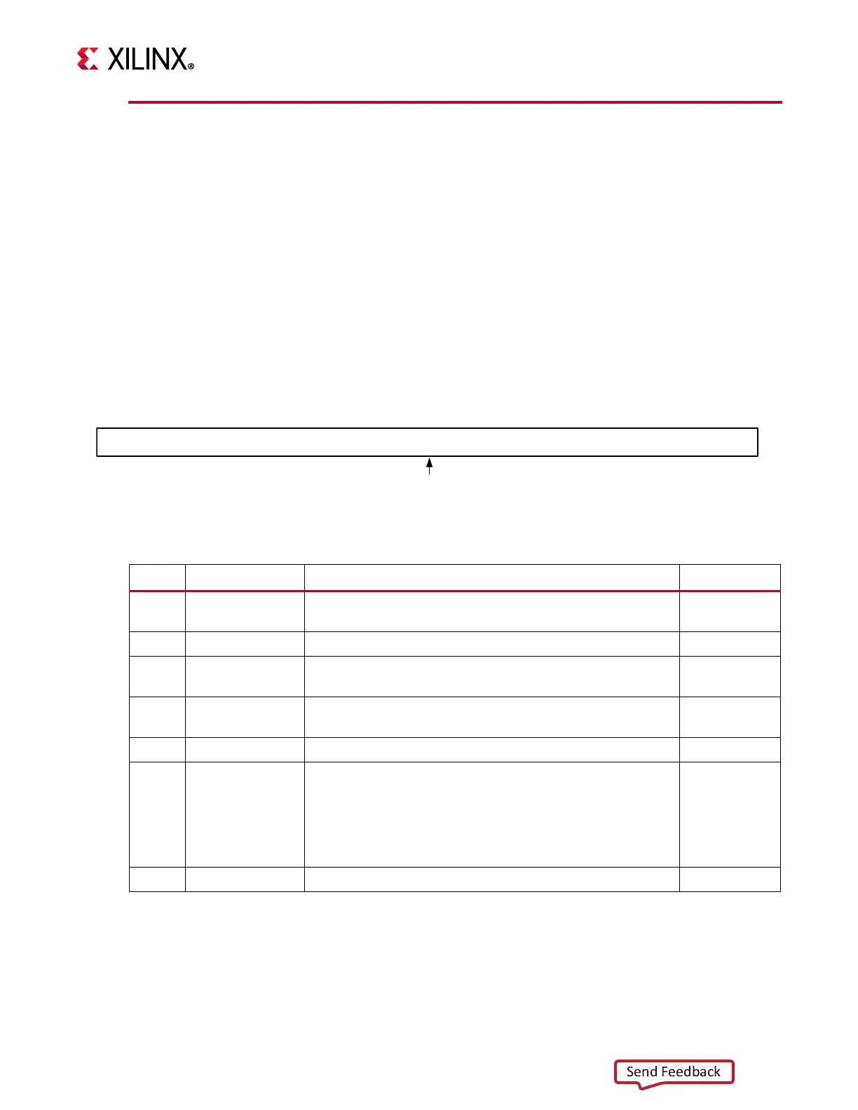
X-Ref Target - Figure 2-2
Figure 2-2: R0-R31
R0 – R31
0 31
X19739-091117
Table 2-7: General Purpose Registers (R0-R31)
Bits Name Description Reset Value
0:31 R0 Always has a value of zero. Anything written to R0 is
discarded
0x00000000
0:31 R1 through R13 32-bit general purpose registers -
0:31 R14 32-bit register used to store return addresses for
interrupts.
-
0:31 R15 32-bit general purpose register. Recommended for storing
return addresses for user vectors.
-
0:31 R16 32-bit register used to store return addresses for breaks. -
0:31 R17 If MicroBlaze is configured to support hardware
exceptions, this register is loaded with the address of the
instruction following the instruction causing the HW
exception, except for exceptions in delay slots that use BTR
instead (see
Branch Target Register (BTR)); if not, it is a
general purpose register.
-
0:31 R18 through R31 R18 through R31 are 32-bit general purpose registers. -