MicroBlaze Processor Reference Guide 95
UG984 (v2018.2) June 21, 2018 www.xilinx.com
Chapter 2: MicroBlaze Architecture
Stream Link Interfaces
MicroBlaze can be configured with up to 16 AXI4-Stream interfaces, each consisting of one
input and one output port. The channels are dedicated uni-directional point-to-point data
streaming interfaces.
For detailed information on the AXI4-Stream interface, please refer to the AMBA 4 AXI4-
Stream Protocol Specification, Version 1.0 (
Arm IHI 0051A) [Ref 14] document.
The interfaces on MicroBlaze are 32 bits wide. A separate bit indicates whether the
sent/received word is of control or data type. The get instruction in the MicroBlaze ISA is
used to transfer information from a port to a general purpose register. The put instruction
is used to transfer data in the opposite direction. Both instructions come in 4 flavors:
blocking data, non-blocking data, blocking control, and non-blocking control. For a
detailed description of the get and put instructions, see
Chapter 5, MicroBlaze Instruction
Set Architecture.
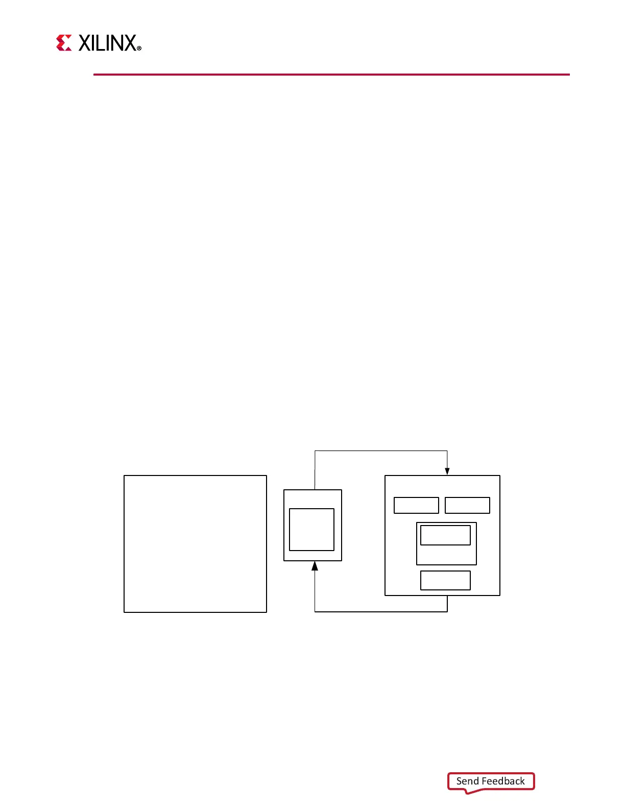
Hardware Acceleration
Each link provides a low latency dedicated interface to the processor pipeline. Thus they are
ideal for extending the processors execution unit with custom hardware accelerators. A
simple example is illustrated in the following figure. The code uses RFSLx to indicate the
used link.
This method is similar to extending the ISA with custom instructions, but has the benefit of
not making the overall speed of the processor pipeline dependent on the custom function.
Also, there are no additional requirements on the software tool chain associated with this
type of functional extension.
X-Ref Target - Figure 2-25
Figure 2-25: Stream Link Used with HW Accelerated Function f
x
MicroBlaze
Link x
// Configure fx
cput Rc, RFSLx
// Store operands
put Ra, RFSLx // op 1
put Rb, RFSLx // op 2
// Load result
Register
File
Custom HW Accelerator
Op 1 Reg Op 2 Reg
ConfigReg
f
x
Result Reg
Link x
X19783-091317