MicroBlaze Processor Reference Guide 137
UG984 (v2018.2) June 21, 2018 www.xilinx.com
Chapter 3: MicroBlaze Signal Interface Description
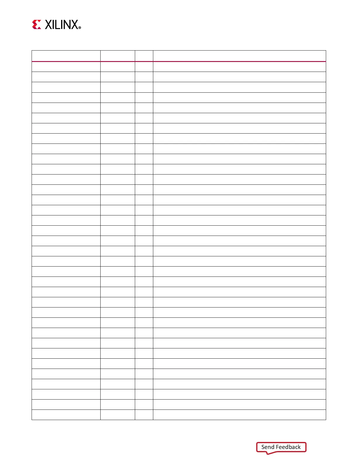
Table 3-1: Summary of MicroBlaze Core I/O
Signal Interface I/O Description
M_AXI_DP_AWID
M_AXI_DP O
Master Write address ID
M_AXI_DP_AWADDR
M_AXI_DP O
Master Write address
M_AXI_DP_AWLEN
M_AXI_DP O
Master Burst length
M_AXI_DP_AWSIZE
M_AXI_DP O
Master Burst size
M_AXI_DP_AWBURST
M_AXI_DP O
Master Burst type
M_AXI_DP_AWLOCK
M_AXI_DP O
Master Lock type
M_AXI_DP_AWCACHE
M_AXI_DP O
Master Cache type
M_AXI_DP_AWPROT
M_AXI_DP O
Master Protection type
M_AXI_DP_AWQOS
M_AXI_DP O
Master Quality of Service
M_AXI_DP_AWVALID
M_AXI_DP O
Master Write address valid
M_AXI_DP_AWREADY
M_AXI_DP I
Slave Write address ready
M_AXI_DP_WDATA
M_AXI_DP O
Master Write data
M_AXI_DP_WSTRB
M_AXI_DP O
Master Write strobes
M_AXI_DP_WLAST
M_AXI_DP O
Master Write last
M_AXI_DP_WVALID
M_AXI_DP O
Master Write valid
M_AXI_DP_WREADY
M_AXI_DP I
Slave Write ready
M_AXI_DP_BID
M_AXI_DP I
Slave Response ID
M_AXI_DP_BRESP
M_AXI_DP I
Slave Write response
M_AXI_DP_BVALID
M_AXI_DP I
Slave Write response valid
M_AXI_DP_BREADY
M_AXI_DP O
Master Response ready
M_AXI_DP_ARID
M_AXI_DP O
Master Read address ID
M_AXI_DP_ARADDR
M_AXI_DP O
Master Read address
M_AXI_DP_ARLEN
M_AXI_DP O
Master Burst length
M_AXI_DP_ARSIZE
M_AXI_DP O
Master Burst size
M_AXI_DP_ARBURST
M_AXI_DP O
Master Burst type
M_AXI_DP_ARLOCK
M_AXI_DP O
Master Lock type
M_AXI_DP_ARCACHE
M_AXI_DP O
Master Cache type
M_AXI_DP_ARPROT
M_AXI_DP O
Master Protection type
M_AXI_DP_ARQOS
M_AXI_DP O
Master Quality of Service
M_AXI_DP_ARVALID
M_AXI_DP O
Master Read address valid
M_AXI_DP_ARREADY
M_AXI_DP I
Slave Read address ready
M_AXI_DP_RID
M_AXI_DP I
Slave Read ID tag
M_AXI_DP_RDATA
M_AXI_DP I
Slave Read data
M_AXI_DP_RRESP
M_AXI_DP I
Slave Read response
M_AXI_DP_RLAST
M_AXI_DP I
Slave Read last