MicroBlaze Processor Reference Guide 190
UG984 (v2018.2) June 21, 2018 www.xilinx.com
Chapter 4: MicroBlaze Application Binary Interface
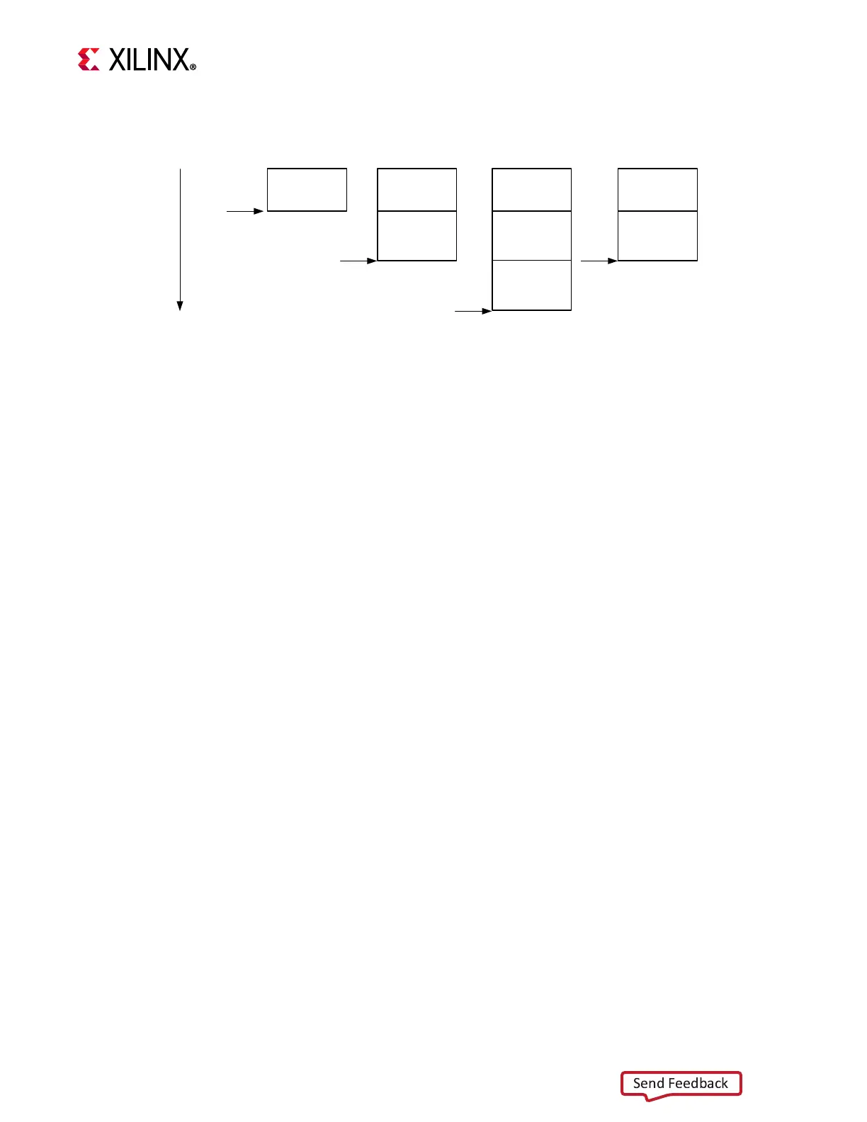
Details of how the stack is maintained are shown in the following figure.
Stack protection is available to ensure that the stack does not grow above the high limit or
shrink below the low limit. The Stack High Register (SHR) and Stack Low Register (SLR) are
used to enforce this, respectively. These registers are automatically initialized to the stack
limits from linker symbols by the crt0.o initialization file.
Enabling stack protection in hardware can be useful to detect erroneous program behavior
due to stack size issues, which can otherwise be very hard to debug.
Calling Convention
The caller function passes parameters to the callee function using either the registers (R5
through R10) or on its own stack frame. The callee uses the stack area of the caller to store
the parameters passed to the callee.
See Table 4-1. The parameters for Func 2 are stored either in the registers R5 through R10
or on the stack frame allocated for Func 1.
If Func 2 has more than six integer parameters, the first six parameters can be passed in
registers R5 through R10, whereas all subsequent parameters must be passed on the stack
frame allocated for Func 1, starting at offset SP + 28.
X-Ref Target - Figure 4-1
Figure 4-1: Stack Frame
Func 1
High Memory
SP
Func 1
SP
Func 2
Func 1
SP
Func 2
Func 3
Func 1
SP
Func 2
Low Memory
X19785-082517