MicroBlaze Processor Reference Guide 248
UG984 (v2018.2) June 21, 2018 www.xilinx.com
Chapter 5: MicroBlaze Instruction Set Architecture
lw
Load Word
lw
rD, rA, rB
lwr
rD, rA, rB
lwea
rD, rA, rB
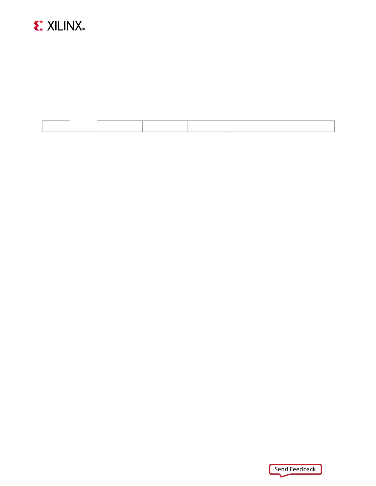
1 1 0 0 1 0 rD rA rB 0 R 0 EA 0 0 0 0 0 0 0
0 6 11 16 21
31
Description
Loads a word (32 bits) from the word aligned memory location that results from adding the contents
of registers rA and rB. The data is placed in register rD.
If the R bit is set, the bytes in the loaded word are reversed , loading data with the opposite
endianness of the endianness defined by the E bit (if virtual protected mode is enabled).
If the EA bit is set, an extended address is used, formed by concatenating rA and rB instead of adding
them.
A data TLB miss exception occurs if virtual protected mode is enabled, and a valid translation entry
corresponding to the address is not found in the TLB.
A data storage exception occurs if access is prevented by a no-access-allowed zone protection. This
only applies to accesses with user mode and virtual protected mode enabled.
An unaligned data access exception occurs if the two least significant bits in the address are not zero.
A privileged instruction error occurs if the EA bit is set, Physical Address Extension (PAE) is enabled,
and the instruction is not explicitly allowed.
Pseudocode
if EA = 1 then
Addr
← (rA) & (rB)
else
Addr ← (rA) + (rB)
if TLB_Miss(Addr) and MSR[VM] = 1 then
ESR[EC]
← 10010;ESR[S]← 0
MSR[UMS] ← MSR[UM]; MSR[VMS] ← MSR[VM]; MSR[UM] ← 0; MSR[VM] ← 0
else if Access_Protected(Addr) and MSR[UM] = 1 and MSR[VM] = 1 then
ESR[EC]
← 10000;ESR[S]← 0; ESR[DIZ] ← 1
MSR[UMS] ← MSR[UM]; MSR[VMS] ← MSR[VM]; MSR[UM] ← 0; MSR[VM] ← 0
else if Addr[30:31]
≠ 0 then
ESR[EC] ← 00001; ESR[W] ← 1; ESR[S] ← 0; ESR[Rx] ← rD
else
(rD)
← Mem(Addr)