MicroBlaze Processor Reference Guide 301
UG984 (v2018.2) June 21, 2018 www.xilinx.com
Chapter 5: MicroBlaze Instruction Set Architecture
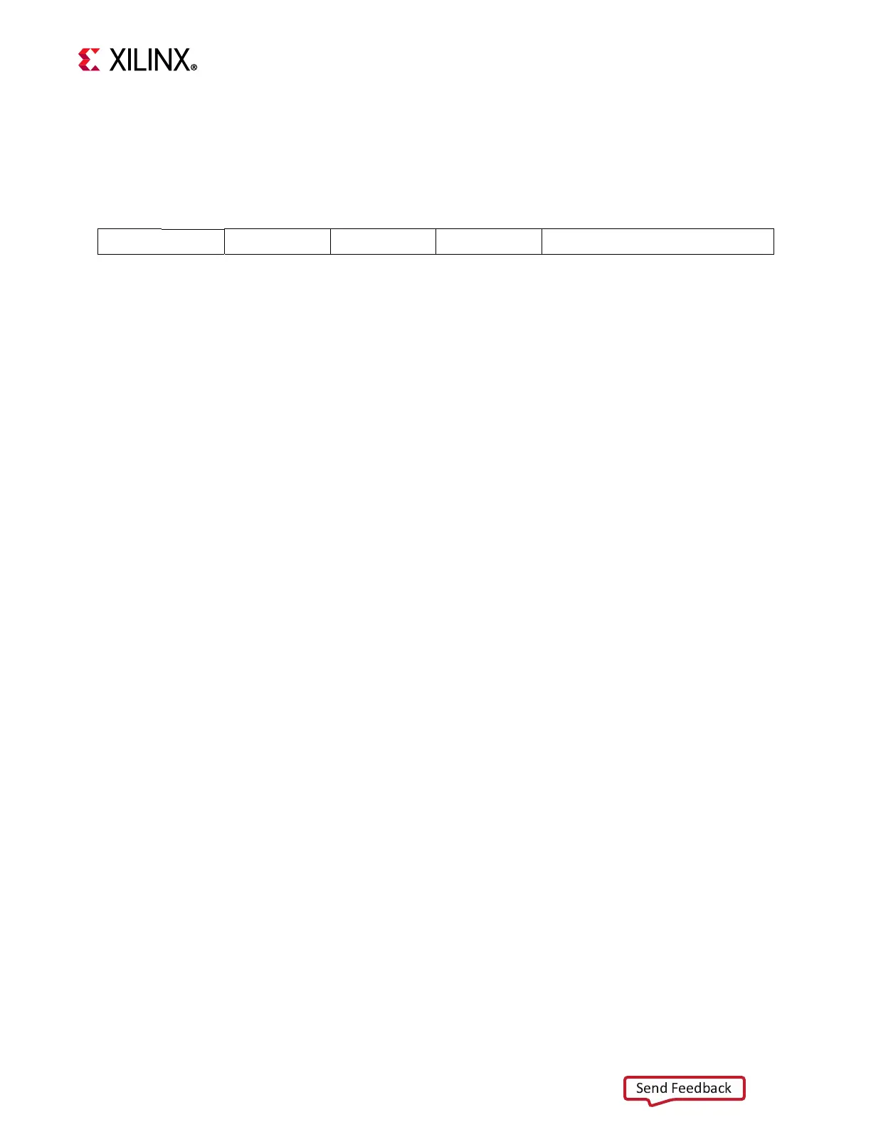
wic
Write to Instruction Cache
wic
rA,rB
1 0 0 1 0 0 0 0 0 0 0 rA rB 0 0 0 0 1 1 0 1 0 0 0
0 6 11 16 21
31
Description
Write into the instruction cache tag to invalidate a cache line. The register rB value is not used.
Register rA contains the address of the affected cache line.
When MicroBlaze is configured to use an MMU (C_USE_MMU >= 1) this instruction is privileged. This
means that if the instruction is attempted in User Mode (MSR[UM] = 1) a Privileged Instruction
exception occurs.
Pseudocode
if MSR[UM] = 1 then
ESR[EC] ← 00111
else
if C_ICACHE_LINE_LEN = 4 then
cacheline_mask
← (1 << log2(C_CACHE_BYTE_SIZE) - 4) - 1
(ICache Line)[((Ra) >> 4) ∧ cacheline_mask].Tag ← 0
if C_ICACHE_LINE_LEN = 8 then
cacheline_mask
← (1 << log2(C_CACHE_BYTE_SIZE) - 5) - 1
(ICache Line)[((Ra) >> 5) ∧ cacheline_mask].Tag ← 0
if C_ICACHE_LINE_LEN = 16 then
cacheline_mask
← (1 << log2(C_CACHE_BYTE_SIZE) - 6) - 1
(ICache Line)[((Ra) >> 6) ∧ cacheline_mask].Tag ← 0
Registers Altered
• ESR[EC], in case a privileged instruction exception is generated
Latency
• 2 cycles
Notes
The WIC instruction is independent of instruction cache enable (MSR[ICE]), and can be used either
with the instruction cache enabled or disabled.
The address of the affected cache line is the virtual address when the parameter C_USE_MMU = 3
(VIRTUAL) and the MMU is in virtual mode, otherwise it is the physical address.