MicroBlaze Processor Reference Guide 53
UG984 (v2018.2) June 21, 2018 www.xilinx.com
Chapter 2: MicroBlaze Architecture
clearing the BTC, the memory barrier or synchronizing branch should not be placed
immediately after a branch instruction.
There are three cases where the branch prediction can cause a mispredict, namely:
• A conditional branch that should not have been taken, is actually taken,
• A conditional branch that should actually have been taken, is not taken,
• The target address of a return instruction is incorrect, which might occur when
returning from a function called from different places in the code.
All of these cases are detected and corrected when the branch or return instruction reaches
the execute stage, and the branch prediction bits or target address are updated in the BTC,
to reflect the actual instruction behavior. This correction incurs a penalty of 2 clock cycles
for the 5-stage pipeline and 7-9 clock cycles for the 8-stage pipeline.
The size of the BTC can be selected with C_BRANCH_TARGET_CACHE_SIZE. The default
recommended setting uses one block RAM, and provides 512 entries. When selecting 64
entries or below, distributed RAM is used to implement the BTC, otherwise block RAM is
used.
When the BTC uses block RAM, and C_FAULT_TOLERANT is set to 1, block RAMs are
protected by parity. In case of a parity error, the branch is not predicted. To avoid
accumulating errors in this case, the BTC should be cleared periodically by a synchronizing
branch.
The Branch Target Cache is available when C_USE_BRANCH_TARGET_CACHE is set to 1 and
C_AREA_OPTIMIZED is set to 0 (Performance) or 2 (Frequency).
Pipeline Hazard Example
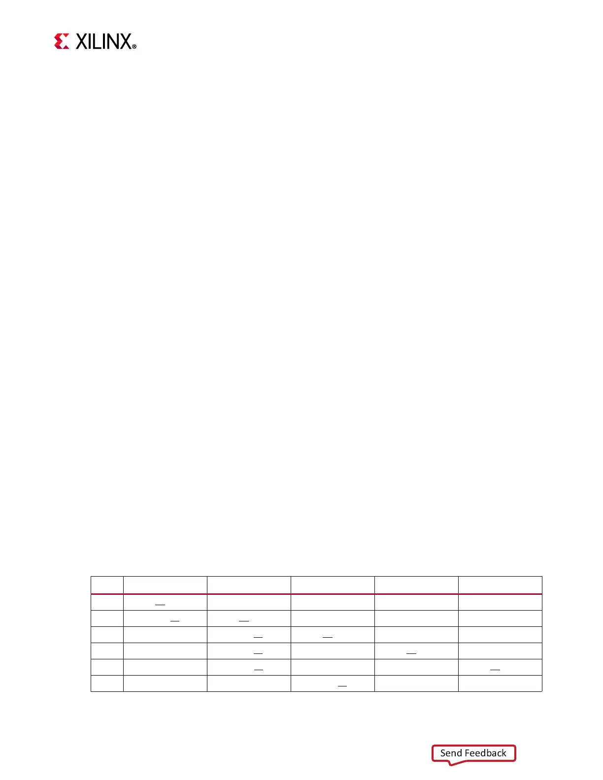
The effect of a data hazard is illustrated in Table 2-37, using the five stage pipeline.
The example shows a data hazard for a multiplication instruction, where the subsequent
add instruction needs the result in register r3 to proceed. This means that the add
instruction is stalled in OF during cycle 3 and 4 until the multiplication is complete.
Table 2-37: Multiplication Data Hazard Example
Cycle IF OF EX MEM WB
1 mul r3, r4, r5
2 add r6, r3, r4 mul r3, r4, r5
3 add r6, r3, r4 mul r3, r4, r5
4 add r6, r3, r4 - mul r3, r4, r5
5 add r6, r3, r4 - - mul r3, r4, r5
6 add r6, r3, r4 - -