MIPI CSI-2 RX Subsystem v4.0 80
PG232 July 02, 2019 www.xilinx.com
Appendix A: Verification, Compliance, and Interoperability
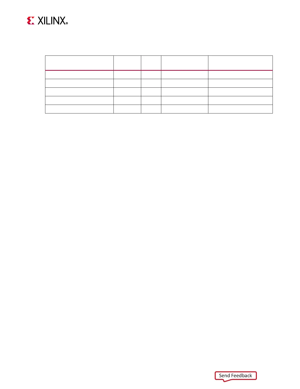
All Xilinx 7 series FPGA loopback designs use the XM107 [Ref 19] loopback card.
Following board guidelines such as equal trace lengths helps in achieving higher line rates.
For PCB guidelines refer to UltraScale Architecture PCB Design User Guide (UG583) [Ref 17].
Table A-4: Loopback Testing with Xilinx 7 Series FPGA Devices
Board/Device Line Rate Lanes Calibration Mode
Clock Selection
(C_EN_CLK300M)
AC701/ xc7a200tfbg676-2 1250 4 Auto False
KC705/ xc7k325tffg900-2 1250 4 Auto False
VC709/ xc7vx690tffg1761-2 1250 4 Auto False
ZC702/ xc7z020clg484-1 928 4 Auto True
ZC706/ xc7z045ffg900-2 1250 4 Auto True
 Loading...