ZCU106 Board User Guide 106
UG1244 (v1.0) March 28, 2018 www.xilinx.com
Chapter 3: Board Component Descriptions
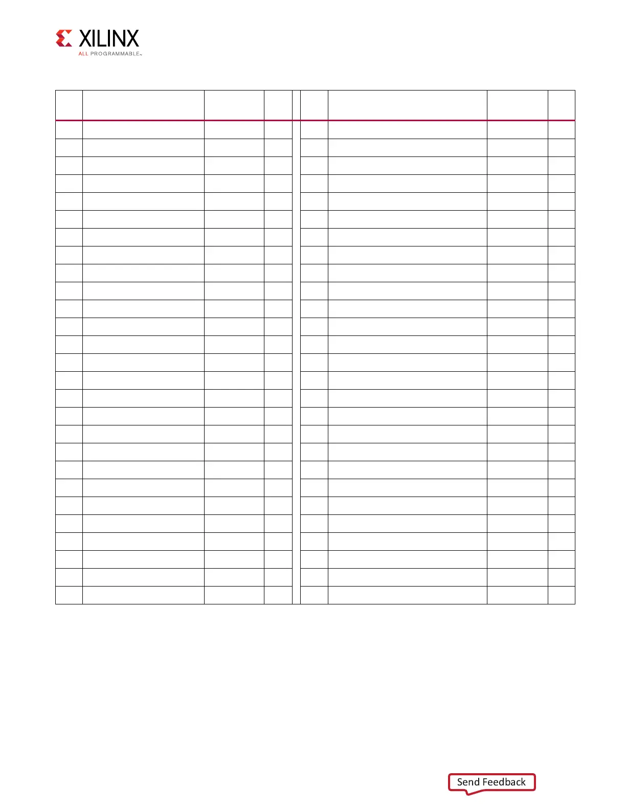
Table 3-44: J5 HPC0 FMC Section C and D Connections to XCZU7EV U1
J5
Pin
Schematic Net Name
I/O
Standard
U1
Pin
J5
Pin
Schematic Net Name
I/O
Standard
U1
Pin
C2 FMC_HPC0_DP0_C2M_P
(7)
R6 D1 VADJ_FMC_PGOOD (6)
C3 FMC_HPC0_DP0_C2M_N
(7)
R5 D4 FMC_HPC0_GBTCLK0_M2C_P (1)
(1)(7)
V8
C6 FMC_HPC0_DP0_M2C_P
(7)
R2 D5 FMC_HPC0_GBTCLK0_M2C_N (1)
(1)(7)
V7
C7 FMC_HPC0_DP0_M2C_N
(7)
R1 D8 FMC_HPC0_LA01_CC_P LVCMOS18 H18
C10 FMC_HPC0_LA06_P LVCMOS18 H19 D9 FMC_HPC0_LA01_CC_N LVCMOS18 H17
C11 FMC_HPC0_LA06_N LVCMOS18 G19 D11 FMC_HPC0_LA05_P LVCMOS18 K17
C14 FMC_HPC0_LA10_P LVCMOS18 L15 D12 FMC_HPC0_LA05_N LVCMOS18 J17
C15 FMC_HPC0_LA10_N LVCMOS18 K15 D14 FMC_HPC0_LA09_P LVCMOS18 H16
C18 FMC_HPC0_LA14_P LVCMOS18 C13 D15 FMC_HPC0_LA09_N LVCMOS18 G16
C19 FMC_HPC0_LA14_N LVCMOS18 C12 D17 FMC_HPC0_LA13_P LVCMOS18 G15
C22 FMC_HPC0_LA18_CC_P LVCMOS18 D11 D18 FMC_HPC0_LA13_N LVCMOS18 F15
C23 FMC_HPC0_LA18_CC_N LVCMOS18 D10 D20 FMC_HPC0_LA17_CC_P LVCMOS18 F11
C26 FMC_HPC0_LA27_P LVCMOS18 A8 D21 FMC_HPC0_LA17_CC_N LVCMOS18 E10
C27 FMC_HPC0_LA27_N LVCMOS18 A7 D23 FMC_HPC0_LA23_P LVCMOS18 B11
C30 FMC_HPC0_IIC_SCL
(2)
D24 FMC_HPC0_LA23_N LVCMOS18 A11
C31 FMC_HPC0_IIC_SDA
(2)
D26 FMC_HPC0_LA26_P LVCMOS18 B9
C34 GND D27 FMC_HPC0_LA26_N LVCMOS18 B8
C35 VCC12_SW D29 FMC_HPC0_TCK_BUF
(3)
C37 VCC12_SW D30 FPGA_TDO_FMC_TDI_BUF
(4)
C39 UTIL_3V3 D31 FMC_HPC0_TDO_HPC1_TDI
(3)(4)
D32 UTIL_3V3_10A
D33 FMC_HPC0_TMS_BUF
(3)
D34 NC
D35 GND
D36 UTIL_3V3
D38 UTIL_3V3
D40 UTIL_3V3
Notes:
1. Series capacitor coupled to FPGA U1 pin.
2. Connected to I2C switch U135 pins 4 and 5.
3. FPGA U1 JTAG TCK, TMS, TDO pins are buffered by U48 SN74AVC8T245.
4. J5 HPC0 TDO-TDI connections to U27 HPC0 FMC JTAG bypass switch (N.C. normally-closed/bypassing J5 until an FMC card is
plugged onto J5).
5. FMC_HPC0_PRSNT_M2C_B is the HPC FMC JTAG bypass switch U27.4 OE control signal, driven by I2C I/O expander U97.13.
6. Sourced from VADJ_FMC_BUS voltage regulator U63 MAX15301 pin 32 power good output signal.
7. U1 MGT (I/O standards do not apply).

 Loading...


