ZCU106 Board User Guide 105
UG1244 (v1.0) March 28, 2018 www.xilinx.com
Chapter 3: Board Component Descriptions
The ZCU106 board FMC VADJ voltage VADJ_FMC_BUS for the J5 (HPC0) and J4 (HPC1) FMC
connectors is determined by the MAX15301 U63 voltage regulator described in Board
Power System, page 122. The valid values of the VADJ_FMC rail are 1.2V, 1.5V, and 1.8V. The
HPC0 J5 connections to XCZU7EV U1 are shown in Table 3-43 through Table 3-46.
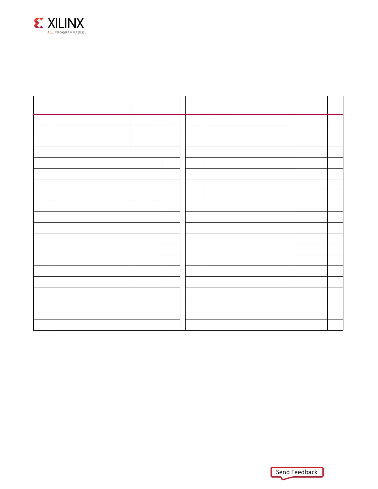
Table 3-43: J5 HPC0 FMC Section A and B Connections to XCZU7EV U1
J5 Pin Schematic Net Name
I/O
Standard
U1
Pin
J5 Pin Schematic Net Name
I/O
Standard
U1
Pin
A2 FMC_HPC0_DP1_M2C_P
(7)
U2 B1 NC
A3 FMC_HPC0_DP1_M2C_N
(7)
U1 B4 NC
A6 FMC_HPC0_DP2_M2C_P
(7)
P4 B5 NC
A7 FMC_HPC0_DP2_M2C_N
(7)
P3 B8 NC
A10 FMC_HPC0_DP3_M2C_P
(7)
V4 B9 NC
A11 FMC_HPC0_DP3_M2C_N
(7)
V3 B12 FMC_HPC0_DP7_M2C_P
(7)
J2
A14 FMC_HPC0_DP4_M2C_P
(7)
G2 B13 FMC_HPC0_DP7_M2C_N
(7)
J1
A15 FMC_HPC0_DP4_M2C_N
(7)
G1 B16 FMC_HPC0_DP6_M2C_P
(7)
N2
A18 FMC_HPC0_DP5_M2C_P
(7)
L2 B17 FMC_HPC0_DP6_M2C_N
(7)
N1
A19 FMC_HPC0_DP5_M2C_N
(7)
L1 B20 FMC_HPC0_GBTCLK1_M2C_P
(1)(7)
T8
A22 FMC_HPC0_DP1_C2M_P
(7)
T4 B21 FMC_HPC0_GBTCLK1_M2C_N
(1)(7)
T7
A23 FMC_HPC0_DP1_C2M_N
(7)
T3 B24 NC
A26 FMC_HPC0_DP2_C2M_P
(7)
N6 B25 NC
A27 FMC_HPC0_DP2_C2M_N
(7)
N5 B28 NC
A30 FMC_HPC0_DP3_C2M_P
(7)
U6 B29 NC
A31 FMC_HPC0_DP3_C2M_N
(7)
U5 B32 FMC_HPC0_DP7_C2M_P
(7)
K4
A34 FMC_HPC0_DP4_C2M_P
(7)
H4 B33 FMC_HPC0_DP7_C2M_N
(7)
K3
A35 FMC_HPC0_DP4_C2M_N
(7)
H3 B36 FMC_HPC0_DP6_C2M_P
(7)
M4
A38 FMC_HPC0_DP5_C2M_P
(7)
L6 B37 FMC_HPC0_DP6_C2M_N
(7)
M3
A39 FMC_HPC0_DP5_C2M_N
(7)
L5 B40 NC
Notes:
1. Series capacitor coupled to FPGA U1 pin.
2. Connected to I2C switch U135 pins 4 and 5.
3. FPGA U1 JTAG TCK, TMS, TDO pins are buffered by U48 SN74AVC8T245.
4. J5 HPC0 TDO-TDI connections to U27 HPC0 FMC JTAG bypass switch (N.C. normally-closed/bypassing J5 until an FMC card
is plugged onto J5).
5. FMC_HPC0_PRSNT_M2C_B is the HPC FMC JTAG bypass switch U27.4 OE control signal, driven by I2C I/O expander U97.13.
6. Sourced from VADJ_FMC_BUS voltage regulator U63 MAX15301 pin 32 power good output signal.
7. U1 MGT (I/O standards do not apply).

 Loading...


