ZCU106 Board User Guide 113
UG1244 (v1.0) March 28, 2018 www.xilinx.com
Chapter 3: Board Component Descriptions
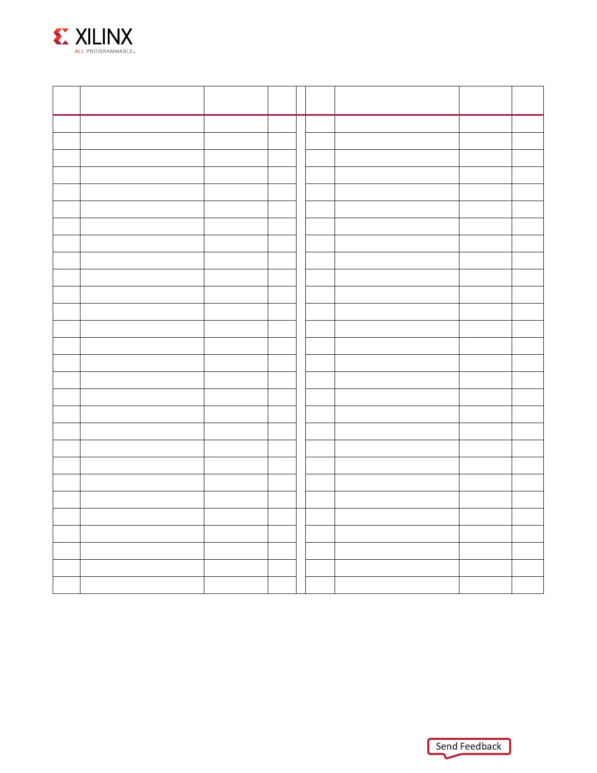
Table 3-51: J4 HPC1 FMC Section G and H Connections to XCZU7EV U1
J4
Pin
Schematic Net Name I/O Standard
U1
Pin
J4
Pin
Schematic Net Name
I/O
Standard
U1
Pin
G2 FMC_HPC1_CLK1_M2C_P LVDS H1 NC
G3 FMC_HPC1_CLK1_M2C_N LVDS H2 FMC_HPC1_PRSNT_M2C_B
(1)
G6 FMC_HPC1_LA00_CC_P LVDS B18 H4 FMC_HPC1_CLK0_M2C_P LVDS F23
G7 FMC_HPC1_LA00_CC_N LVDS B19 H5 FMC_HPC1_CLK0_M2C_N LVDS E23
G9 FMC_HPC1_LA03_P LVDS J21 H7 FMC_HPC1_LA02_P LVDS K22
G10 FMC_HPC1_LA03_N LVDS J22 H8 FMC_HPC1_LA02_N LVDS K23
G12 FMC_HPC1_LA08_P LVDS J25 H10 FMC_HPC1_LA04_P LVDS J24
G13 FMC_HPC1_LA08_N LVDS H26 H11 FMC_HPC1_LA04_N LVDS H24
G15 FMC_HPC1_LA12_P LVDS E19 H13 FMC_HPC1_LA07_P LVDS D22
G16 FMC_HPC1_LA12_N LVDS D19 H14 FMC_HPC1_LA07_N LVDS C23
G18 FMC_HPC1_LA16_P LVDS C18 H16 FMC_HPC1_LA11_P LVDS A20
G19 FMC_HPC1_LA16_N LVDS C19 H17 FMC_HPC1_LA11_N LVDS A21
G21 NC H19 FMC_HPC1_LA15_P LVDS A18
G22 NC H20 FMC_HPC1_LA15_N LVDS A19
G24 NC H22 NC
G25 NC H23 NC
G27 NC H25 NC
G28 NC H26 NC
G30 NC H28 NC
G31 NC H29 NC
G33 NC H31 NC
G34 NC H32 NC
G36 NC H34 NC
G37 NC H35 NC
G39 VADJ_FMC_BUS H37 NC
H38 NC
H40 VADJ_FMC_BUS
Notes:
1. FMC_HPC1_PRSNT_M2C_B is the HPC FMC JTAG bypass switch U24.4 OE control signal is driven from I2C I/O expander
U97.14.

 Loading...


