Zynq-7000 PCB Design Guide www.xilinx.com 49
UG933 (v1.8) November 7, 2014
Chapter 4: SelectIO Signaling
external precision resistors placed on the VRN and VRP pins for that bank, the resulting
controlled output impedance for that bank would be 50Ω. If 100Ω resistors were already
required on the VRN and VRP pins (for the purpose of creating a Thevenin-equivalent split
termination circuit equal to 50Ω), and a 50Ω controlled impedance driver was required in
the same bank, this could be accomplished by using the “DIV2” versions of the drivers, such
as LVDCI_DIV2_15 (Figure 4-9 and Figure 4-10). Weak LVCMOS drivers of 6mA to 8mA
drive strength have an output impedance approximately equal to 50Ω (Figure 4-11).
Parallel terminations have the best performance when V
TT
(the voltage source connected to
the parallel termination resistor) is equal to half of the signaling voltage, since this is
typically the center voltage of the data eye. For 2.5V signals (V
CCO
= 2.5V), V
TT
is ideally
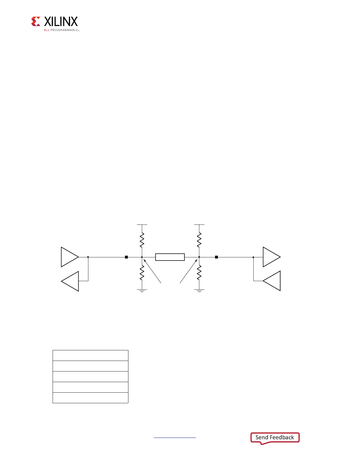
1.25V. In cases where this voltage is not available, it is advisable to use a Thevenin parallel
termination. Thevenin parallel termination consists of a voltage divider with a parallel
resistance equal to the characteristic impedance of the transmission line (50Ω in most
cases). The divided voltage point is designed to be at V
TT
. Figure 4-12 illustrates a Thevenin
parallel termination powered from 2.5V V
CCO
, made up of two 100Ω resistors, resulting in a
V
TT
of 1.25V and a parallel equivalent resistance (R
PEQ
) of 50Ω .
Parallel termination can be less desirable than series termination or controlled-impedance
drivers because it dissipates more power. This trade-off must be weighed against other
trade-offs to determine the optimum termination topography for an interface.
Table 4-3 lists example I/O interface types that can be used with the bidirectional
point-to-point topography.
X-Ref Target - Figure 4-12
Figure 4-12: Thevenin Parallel Termination (Bidirectional Point-to-Point Topography)
UG933_c4_12_031711
R
PT
= 2 x Z
0
= 100Ω R
PT
= 2 x Z
0
= 100Ω
R
PT
= 2 x Z
0
= 100ΩR
PT
= 2 x Z
0
= 100Ω
V
CCO
= 2.5V
V
TTEQ
= 1.25V
V
CCO
= 2.5V
Z
0
= 50Ω
R
O
= 25Ω
R
O
= 25Ω
Table 4-3: Example I/O Interface Types for Bidirectional Point-to-Point I/O Topographies
LVTTL
LVC MOS
LVDCI
HSLVDCI
SSTL15
 Loading...


