AD9361 Reference Manual UG-570
| Page 115 of 128
Figu
re 82. Nominal Timing Diagram, SPI Write
Figu
re 83. Nominal Timing Diagram, SPI Read
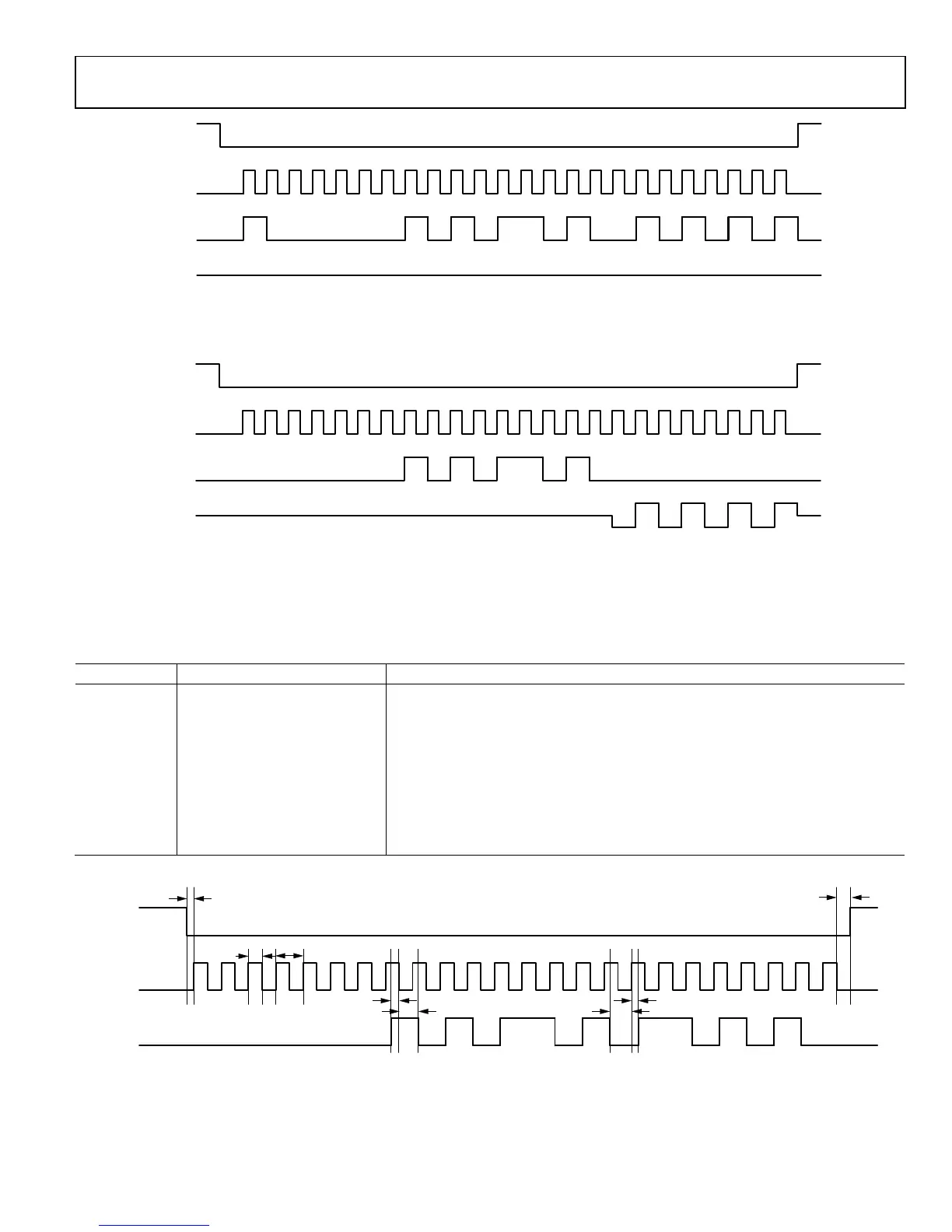
Table 53 lists the timing specifications for the SPI bus. The relationship between these parameters is shown in Figure 84. This diagram
shows a 3-wire SPI bus timing diagram with these parameters marked. Note that this is a single read operation, so the bus-ready
parameter after the data is driven from the AD9361 is not shown in the diagram.
Table 53. SPI Bus Timing Constraint Values
Parameter Min Typ Max Description
t
CP
20 ns SPI_CLK cycle time (clock period)
t
MP
9 ns SPI_CLK pulse width
t
SC
1 ns SPI_ENB setup time to first SPI_CLK rising edge
t
HC
0 ns Last SPI_CLK falling edge to SPI_ENB hold
t
S
2 ns SPI_DI data input setup time to SPI_CLK
t
H
1 ns SPI_DI data input hold time to SPI_CLK
t
CO
3 ns 8 ns SPI_CLK rising edge to output data delay (3-wire or 4-wire mode)
t
HZM
t
H
t
CO (max)
Bus turnaround time after BBP drives the last address bit
t
HZS
0 ns t
CO (max)
Bus turnaround time after AD9361 drives the last data bit
Figur
e 84. 3-Wire SPI Timing with Parameter Labels, SPI Read
SPI_ENB
SPI_CLK
SPI_DI
SPI_DO
WRITE TO REGISTER 0x15A, VALUE = 0x55
11668-083
SPI_ENB
SPI_CLK
SPI_DI
SPI_DO
READ REGISTER 0x15A, VALUE = 0x55
11668-084
SPI_ENB
SPI_CLK
SPI_DI
t
MP
t
CP
t
S
t
H
t
SC
t
HC
t
CO
t
HZM
11668-085

 Loading...


