157
2467S–AVR–07/09
ATmega128
8-bit
Timer/Counter
Register
Description
Timer/Counter Control
Register – TCCR2
• Bit 7 – FOC2: Force Output Compare
The FOC2 bit is only active when the WGM20 bit specifies a non-PWM mode. However, for
ensuring compatibility with future devices, this bit must be set to zero when TCCR2 is written
when operating in PWM mode. When writing a logical one to the FOC2 bit, an immediate com-
pare match is forced on the waveform generation unit. The OC2 output is changed according to
its COM21:0 bits setting. Note that the FOC2 bit is implemented as a strobe. Therefore it is the
value present in the COM21:0 bits that determines the effect of the forced compare.
A FOC2 strobe will not generate any interrupt, nor will it clear the Timer in CTC mode using
OCR2 as TOP.
The FOC2 bit is always read as zero.
• Bit 6, 3 – WGM21:0: Waveform Generation Mode
These bits control the counting sequence of the counter, the source for the maximum (TOP)
counter value, and what type of waveform generation to be used. Modes of operation supported
by the Timer/Counter unit are: Normal mode, Clear Timer on Compare match (CTC) mode, and
two types of Pulse Width Modulation (PWM) modes. See Table 64 and “Modes of Operation” on
page 150.
Note: The CTC2 and PWM2 bit definition names are now obsolete. Use the WGM21:0 definitions. How-
ever, the functionality and location of these bits are compatible with previous versions of the timer.
• Bit 5:4 – COM21:0: Compare Match Output Mode
These bits control the Output Compare Pin (OC2) behavior. If one or both of the COM21:0 bits
are set, the OC2 output overrides the normal port functionality of the I/O pin it is connected to.
However, note that the Data Direction Register (DDR) bit corresponding to the OC2 pin must be
set in order to enable the output driver.
When OC2 is connected to the pin, the function of the COM21:0 bits depends on the WGM21:0
bit setting. Table 65 shows the COM21:0 bit functionality when the WGM21:0 bits are set to a
normal or CTC mode (non-PWM).
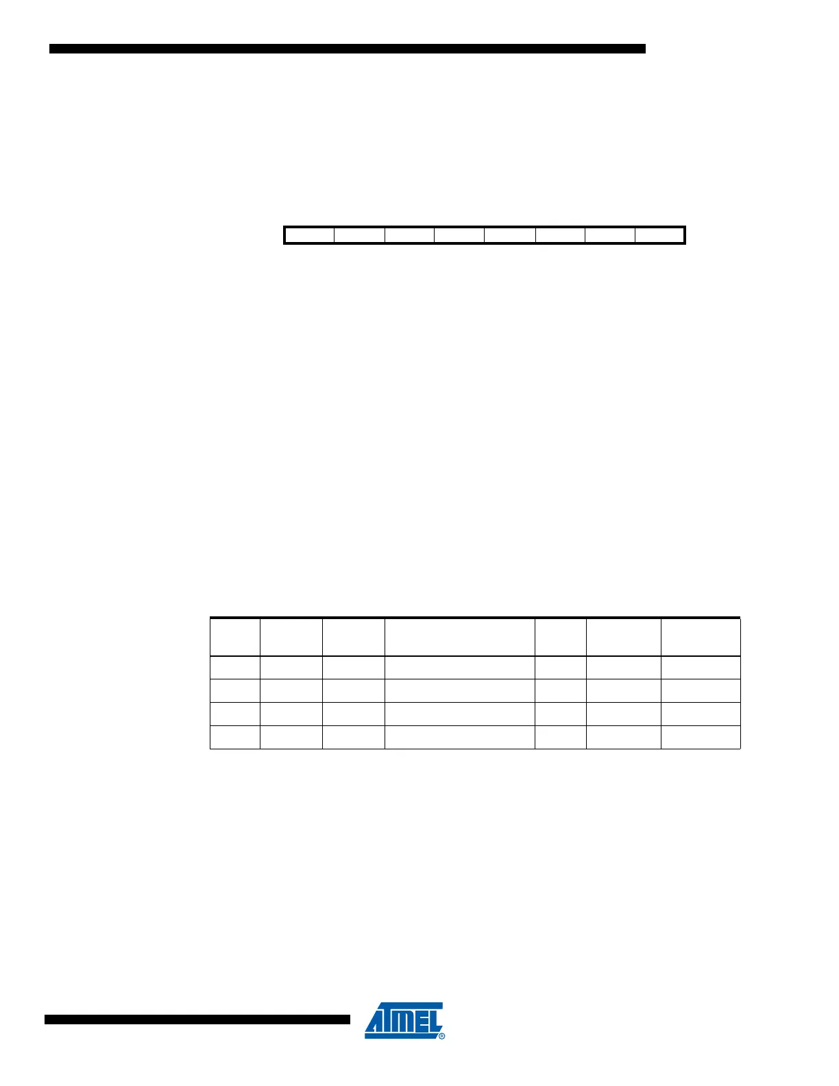
Bit 76543210
FOC2 WGM20 COM21 COM20 WGM21 CS22 CS21 CS20 TCCR2
Read/Write W R/W R/W R/W R/W R/W R/W R/W
Initial Value 0 0 0 0 0 0 0 0
Table 64. Waveform Generation Mode Bit Description
Mode
WGM21
(CTC2)
WGM20
(PWM2)
Timer/Counter Mode
of Operation TOP
Update of
OCR2 at
TOV2 Flag
Set on
0 0 0 Normal 0xFF Immediate MAX
1 0 1 PWM, Phase Correct 0xFF TOP BOTTOM
2 1 0 CTC OCR2 Immediate MAX
3 1 1 Fast PWM 0xFF BOTTOM MAX