227
7647H–AVR–03/12
Atmel ATmega16/32/64/M1/C1
– 1 = Parity error.
This bit is cleared when LERR bit in LINSIR is cleared.
• Bit 1 - LCERR: Checksum Error Flag
–0 = No error,
– 1 = Checksum error.
This bit is cleared when LERR bit in LINSIR is cleared.
• Bit 0 - LBERR: Bit Error Flag
–0 = no error,
– 1 = Bit error.
This bit is cleared when LERR bit in LINSIR is cleared.
17.6.5 LIN Bit Timing Register - LINBTR
• Bit 7 - LDISR: Disable Bit Timing Re synchronization
– 0 = Bit timing re-synchronization enabled (default),
– 1 = Bit timing re-synchronization disabled.
• Bits 5:0 - LBT[5:0]: LIN Bit Timing
Gives the number of samples of a bit.
sample-time = (1 /
fclk
i/o
) x (LDIV[11..0] + 1)
Default value: LBT[6:0]=32 — Min. value: LBT[6:0]=8 — Max. value: LBT[6:0]=63
17.6.6 LIN Baud Rate Register - LINBRR
• Bits 15:12 - Reserved Bits
These bits are reserved for future use. For compatibility with future devices, they must be
written to zero when LINBRR is written.
• Bits 11:0 - LDIV[11:0]: Scaling of clk
i/o
Frequency
The LDIV value is used to scale the entering clk
i/o
frequency to achieve appropriate LIN or
UART baud rate.
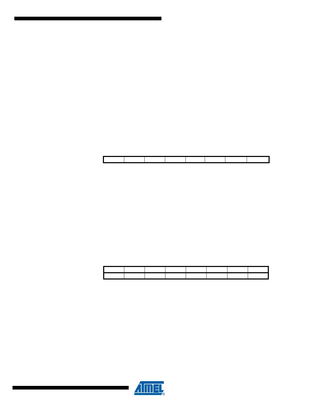
Bit 7654321 0
LDISR - LBT5 LBT4 LBT3 LBT2 LBT1 LBT0
LINBTR
Read/Write R/W R R/(W) R/(W) R/(W) R/(W) R/(W) R/(W)
Initial Value 0 0 1 0 0 0 0 0
Bit 76543210
LDIV7 LDIV6 LDIV5 LDIV4 LDIV3 LDIV2 LDIV1 LDIV0 LINBRRL
----LDIV11LDIV10LDIV9LDIV8LINBRRH
Bit 151413121110 9 8
Read/Write R/W R/W R/W R/W R/W R/W R/W R/W
Initial Value00000000
 Loading...


