EasyManua.ls Logo

Atmel ATmega32M1 User Manual

Atmel ATmega32M1
367 pages
To Next Page IconTo Next Page
To Previous Page IconTo Previous Page
Page #228 background imageLoading...
Page #228 background image
228
7647H–AVR–03/12
Atmel ATmega16/32/64/M1/C1
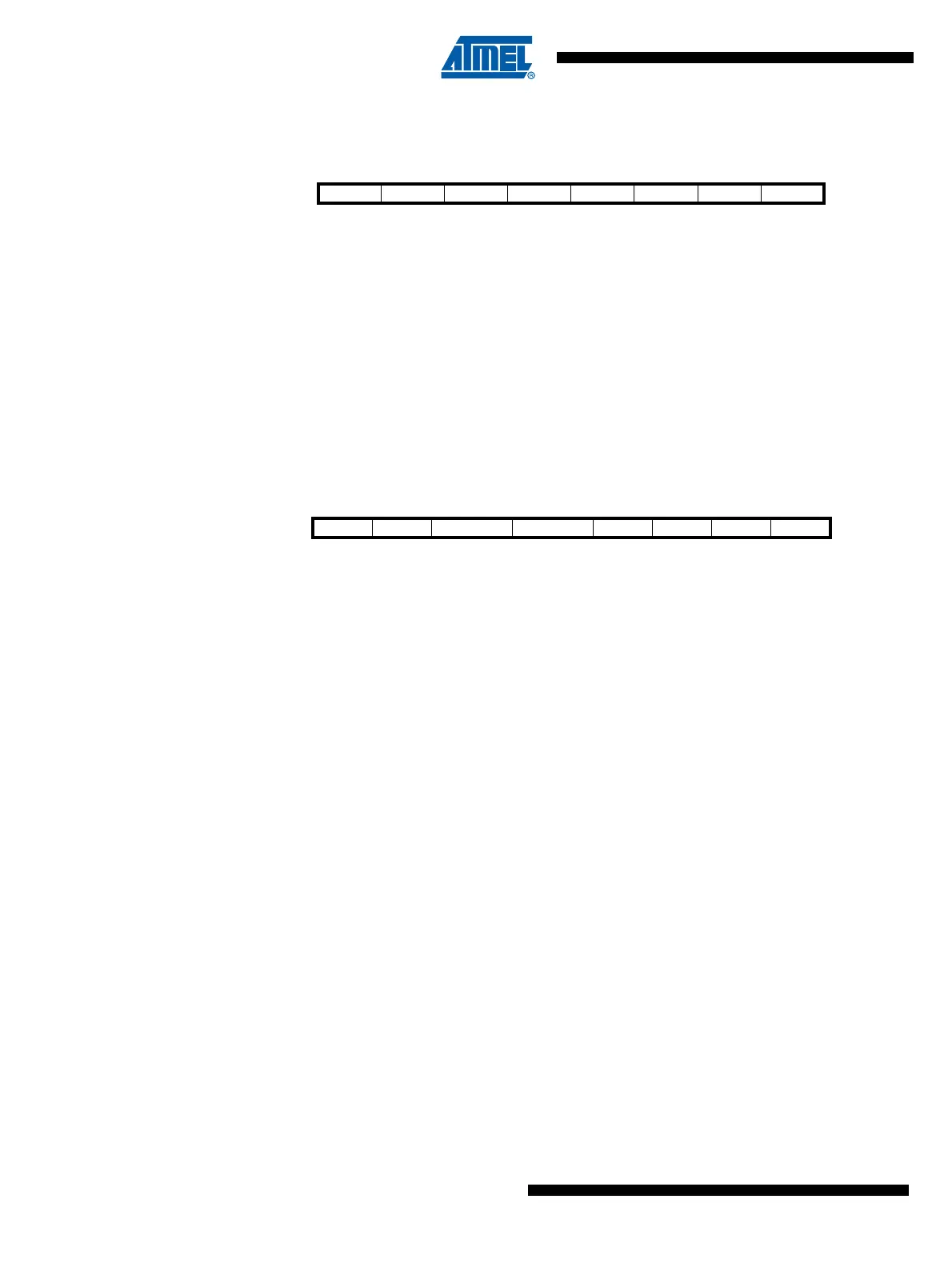
17.6.7 LIN Data Length Register - LINDLR
Bits 7:4 - LTXDL[3:0]: LIN Transmit Data Length
In LIN mode, this field gives the number of bytes to be transmitted (clamped to 8 Max).
In UART mode this field is unused.
Bits 3:0 - LRXDL[3:0]: LIN Receive Data Length
In LIN mode, this field gives the number of bytes to be received (clamped to 8 Max).
In UART mode this field is unused.
17.6.8 LIN Identifier Register - LINIDR
Bits 7:6 - LP[1:0]: Parity
In LIN mode:
LP0 = LID4 ^ LID2 ^ LID1 ^ LID0
LP1 = ! ( LID1 ^ LID3 ^ LID4 ^ LID5 )
In UART mode this field is unused.
Bits 5:4 - LDL[1:0]: LIN 1.3 Data Length
In LIN 1.3 mode:
00 = 2-byte response,
01 = 2-byte response,
10 = 4-byte response,
11 = 8-byte response.
In UART mode this field is unused.
Bits 3:0 - LID[3:0]: LIN 1.3 Identifier
In LIN 1.3 mode: 4-bit identifier.
In UART mode this field is unused.
Bits 5:0 - LID[5:0]: LIN 2.1 Identifier
In LIN 2.1 mode: 6-bit identifier (no length transported).
In UART mode this field is unused.
Bit 76543210
LTXDL3 LTXDL2 LTXDL1 LTXDL0 LRXDL3 LRXDL2 LRXDL1 LRXDL0
LINDLR
Read/Write R/W R/W R/W R/W R/W R/W R/W R/W
Initial Value00000000
Bit 765 43210
LP1 LP0 LID5 / LDL1 LID4 / LDL0 LID3 LID2 LID1 LID0
LINIDR
Read/Write R R R/W R/W R/W R/W R/W R/W
Initial Value 0 0 0 0 0 0 0 0

Table of Contents

Question and Answer IconNeed help?

Do you have a question about the Atmel ATmega32M1 and is the answer not in the manual?

Atmel ATmega32M1 Specifications

General IconGeneral
Architecture8-bit AVR
Flash Memory32 KB
SRAM2 KB
EEPROM1 KB
Clock Speed16 MHz
GPIO Pins32
I/O Pins32
ADC Channels8
ADC Resolution10-bit
UART1
USART1
SPI1
I2C1
PWM Channels6
CAN1
Operating Voltage2.7V - 5.5V
Operating Temperature-40°C to +85°C
Temperature Range-40°C to +85°C
Package44-TQFP, 44-QFN

Summary

Features

AVR CPU Core

Reset and Interrupt Handling

Explanation of interrupt sources, vectors, priority levels, and behavior during interrupt execution.

System Clock

System Clock Prescaler

Details on the CLKPR register for dividing the system clock to reduce power consumption and affect peripheral frequencies.

Power Management and Sleep Modes

8-bit Timer/Counter0 with PWM

Modes of Operation

Detailed explanation of Normal, CTC, and various PWM modes for Timer/Counter0 operation.

Controller Area Network - CAN

CAN Protocol

Explanation of the CAN protocol principles, standards, and message transmission priorities.

Error Management

Description of error detection mechanisms (message and bit level) and fault confinement states.

Analog to Digital Converter - ADC

Features

List of ADC capabilities including resolution, accuracy, conversion time, input channels, and reference voltages.

Starting a Conversion

Procedures for initiating ADC conversions, including single conversion and auto-triggering modes.

debugWIRE On-chip Debug System

Features

Overview of debugWIRE capabilities including program flow control, real-time operation, and symbolic debugging.

Boot Loader Support – Read-While-Write Self-Programming ATmega16/32/64/M1/C1

Self-Programming the Flash

Procedures and considerations for programming the Flash memory using the SPM instruction.

Memory Programming

Electrical Characteristics

Absolute Maximum Ratings*

Critical voltage, current, and temperature limits that must not be exceeded for device reliability.

Instruction Set Summary

Register Summary

Related product manuals