229
7647H–AVR–03/12
Atmel ATmega16/32/64/M1/C1
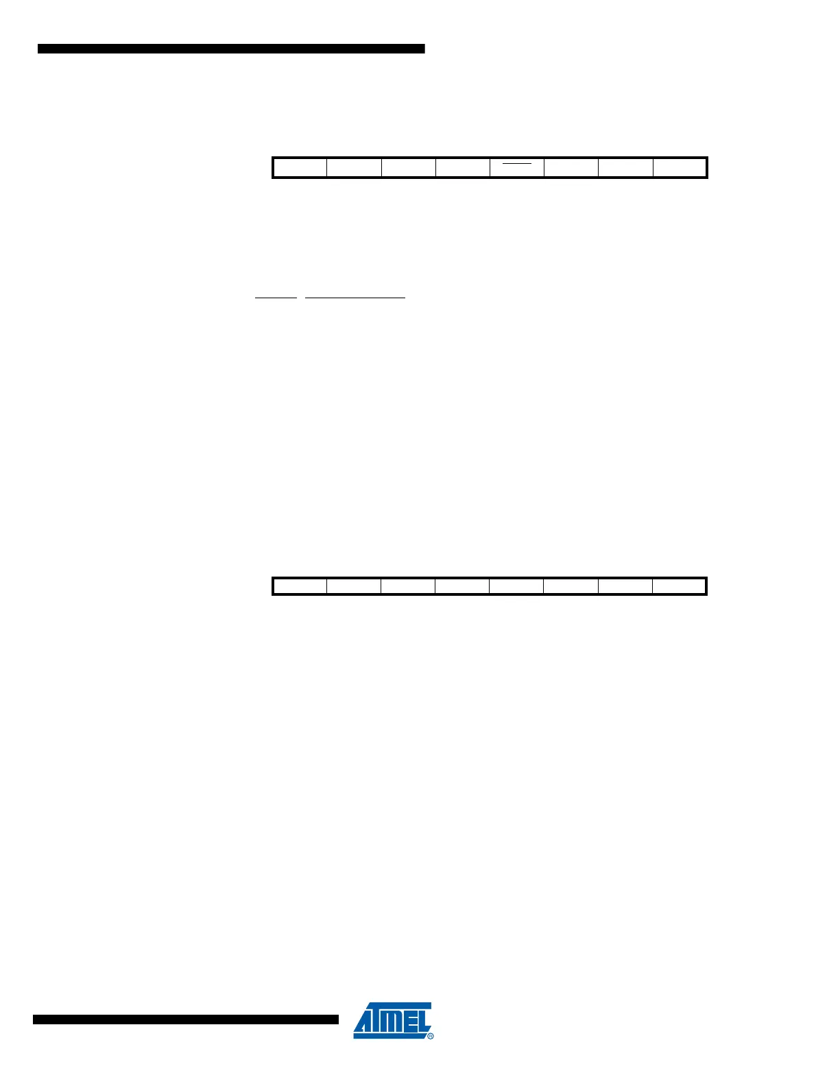
17.6.9 LIN Data Buffer Selection Register - LINSEL
• Bits 7:4 - Reserved Bits
These bits are reserved for future use. For compatibility with future devices, they must be
written to zero when LINSEL is written.
• Bit 3 - LAINC
: Auto Increment of Data Buffer Index
In LIN mode:
– 0 = Auto incrementation of FIFO data buffer index (default),
– 1 = No auto incrementation.
In UART mode this field is unused.
• Bits 2:0 - LINDX 2:0: FIFO LIN Data Buffer Index
In LIN mode: location (index) of the LIN response data byte into the FIFO data buffer. The
FIFO data buffer is accessed through LINDAT.
In UART mode this field is unused.
17.6.10 LIN Data Register - LINDAT
• Bits 7:0 - LDATA[7:0]: LIN Data In / Data out
In LIN mode: FIFO data buffer port.
In UART mode: data register (no data buffer - no FIFO).
– In Write access, data out.
– In Read access, data in.
Bit 76543210
----
LAINC LINDX2 LINDX1 LINDX0 LINSEL
Read/Write----R/WR/WR/WR/W
Initial Value----0000
Bit 76543210
LDATA7 LDATA6 LDATA5 LDATA4 LDATA3 LDATA2 LDATA1 LDATA0 LINDAT
Read/Write R/W R/W R/W R/W R/W R/W R/W R/W
Initial Value00000000