10
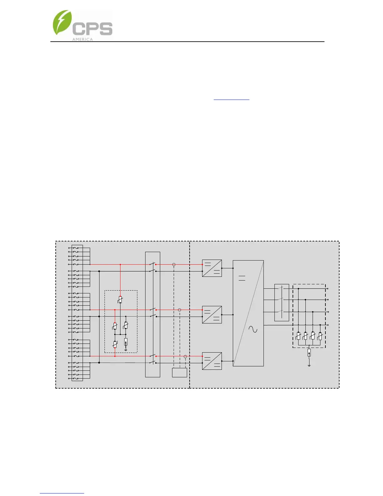
2.5. Schematic Diagram and Circuit Design
The basic electrical schematic diagram of CPS SCA50KTL-DO/US-480 and
SCA60KTL-DO/US-480 inverters are shown in Figure 2-2. The input from PV
source circuits passes through surge protection circuitry, DC EMI wave filters,
and independent DC-DC boost circuitry to achieve maximum power point
tracking and boost the voltages to a common DC bus. The inverter uses line
voltage and frequency measurements to synchronize to the grid and converts
the available PV energy to AC power by injecting balanced 3-phase AC current
into the electric utility grid. Any high frequency AC component is removed by
passing through a two-stage relay and EMI wave filter to produce high quality
AC power.