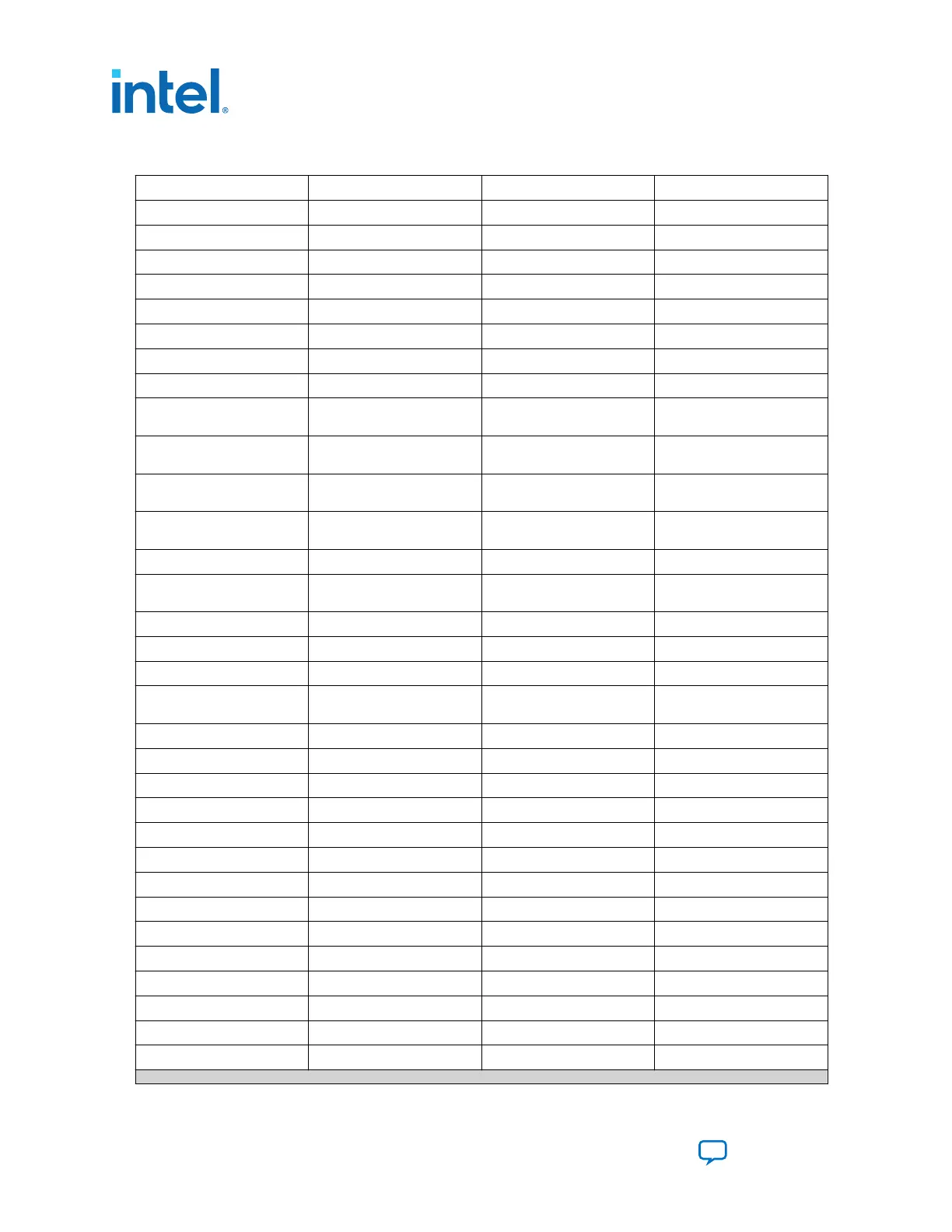
Table 16. MAX V CPLD System Controller Device Pin-Out
Schematic Signal Name Pin Number I/O Standard Description
CLK125_EN E9 2.5 V 125 MHz oscillator enable
CLK50_EN J16 1.8 V 50 MHz oscillator enable
CLK_CONFIG J5 1.8 V Clock Configure
CLK_ENABLE D4 2.5 V Clock Enable
CLK_SEL A2 2.5 V Clock Select
CLOCK_I2C_SCL C12 2.5 V Serial clock line for I
2
C
CLOCK_I2C_SDA C10 2.5 V Serial data line for I
2
C
CPU_RESETN K4 1.8 V FPGA reset push button
FACTORY_LOAD B5 2.5 V DIP switch to load factory or
user design at power-up
FLASH_ADVN N14 1.8 V FSM bus flash memory
address valid
FLASH_CEN0 D14 1.8 V FSM bus flash memory chip
enable
FLASH_CEN1 F11 1.8 V FSM bus flash memory chip
enable
FLASH_CLK N15 1.8 V FSM bus flash memory clock
FLASH_OEN P14 1.8 V FSM bus flash memory
output enable
FLASH_RDYBSYN0 F12 1.8 V FSM bus flash memory ready
FLASH_RDYBSYN1 P15 1.8 V FSM bus flash memory ready
FLASH_RESETN D13 1.8 V FSM bus flash memory reset
FLASH_WEN J1 1.8 V FSM bus flash memory write
enable
FM_A1 F15 1.8 V FM address bus
FM_A2 G16 1.8 V FM address bus
FM_A3 G15 1.8 V FM address bus
FM_A4 H16 1.8 V FM address bus
FM_A5 H15 1.8 V FM address bus
FM_A6 F16 1.8 V FM address bus
FM_A7 G14 1.8 V FM address bus
FM_A8 D16 1.8 V FM address bus
FM_A9 E15 1.8 V FM address bus
FM_A10 E16 1.8 V FM address bus
FM_A11 H14 1.8 V FM address bus
FM_A12 D15 1.8 V FM address bus
FM_A13 F14 1.8 V FM address bus
FM_A14 C14 1.8 V FM address bus
continued...
6. Board Components
683526 | 2023.07.12
Intel
®
Arria
®
10 FPGA Development Kit User Guide
Send Feedback
60