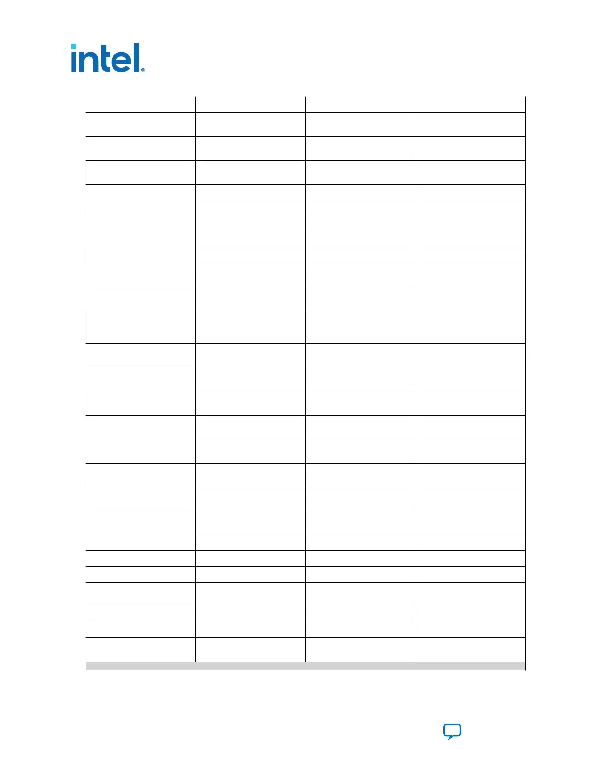
Schematic Signal Name Pin Number I/O Standard Description
MAX_CONF_DONE D7 2.5 V On-board USB-Blaster II
configuration done LED
MAX_ERROR C7 2.5 V FPGA configuration error
LED
MAX_LOAD B6 2.5 V FPGA configuration active
LED
MAX_RESETN J3 1.8 V MAX V reset push button
MSEL0 R12 1.8 V FPGA MSEL0 setting
MSEL1 P11 1.8 V FPGA MSEL1 setting
MSEL2 M11 1.8 V FPGA MSEL2 setting
MV_CLK_50 J12 1.8 V MAX V 50 MHz clock
OVERTEMP E11 2.5 V Temperature monitor fan
enable
OVERTEMPN B16 2.5 V Temperature monitor fan
enable
PGM_CONFIG A6 2.5 V Load the flash memory
image identified by the PGM
LEDs
PGM_LED0 D6 2.5 V Flash memory PGM select
indicator 0
PGM_LED1 C6 2.5 V Flash memory PGM select
indicator 1
PGM_LED2 B7 2.5 V Flash memory PGM select
indicator 2
PGM_SEL A7 2.5 V Toggles the PGM_LED[2:0]
LED sequence
SDI_MF0_BYPASS P13 1.8 V SDI Interface Mode Select
0 / Bypass control
SDI_MF1_AUTO_SLEEP R14 1.8 V SDI Interface Mode Select
1 / Auto Sleep Control
SDI_MF2_MUTE N12 1.8 V SDI Interface Mode Select
2 / Output Mute
SDI_TX_SD_HDN N13 1.8 V SDI Interface TX Signal
Detect
SENSE_CS0N D9 2.5 V SPI Interface Chip Select
SENSE_SCK B9 2.5 V SPI Interface Clock
SENSE_SDI B3 2.5 V SPI Interface Serial Data In
SENSE_SDO C9 2.5 V SPI Interface Serial Data
Out
SENSE_SMB_CLK A15 2.5 V I
2
C Interface Clock
SENSE_SMB_DATA B13 2.5 V I
2
C Interface Data
SI516_FS C5 2.5 V Silicon Labs SI516 Clock
Device Frequency Select
continued...
6. Board Components
683526 | 2023.07.12
Intel
®
Arria
®
10 FPGA Development Kit User Guide
Send Feedback
64