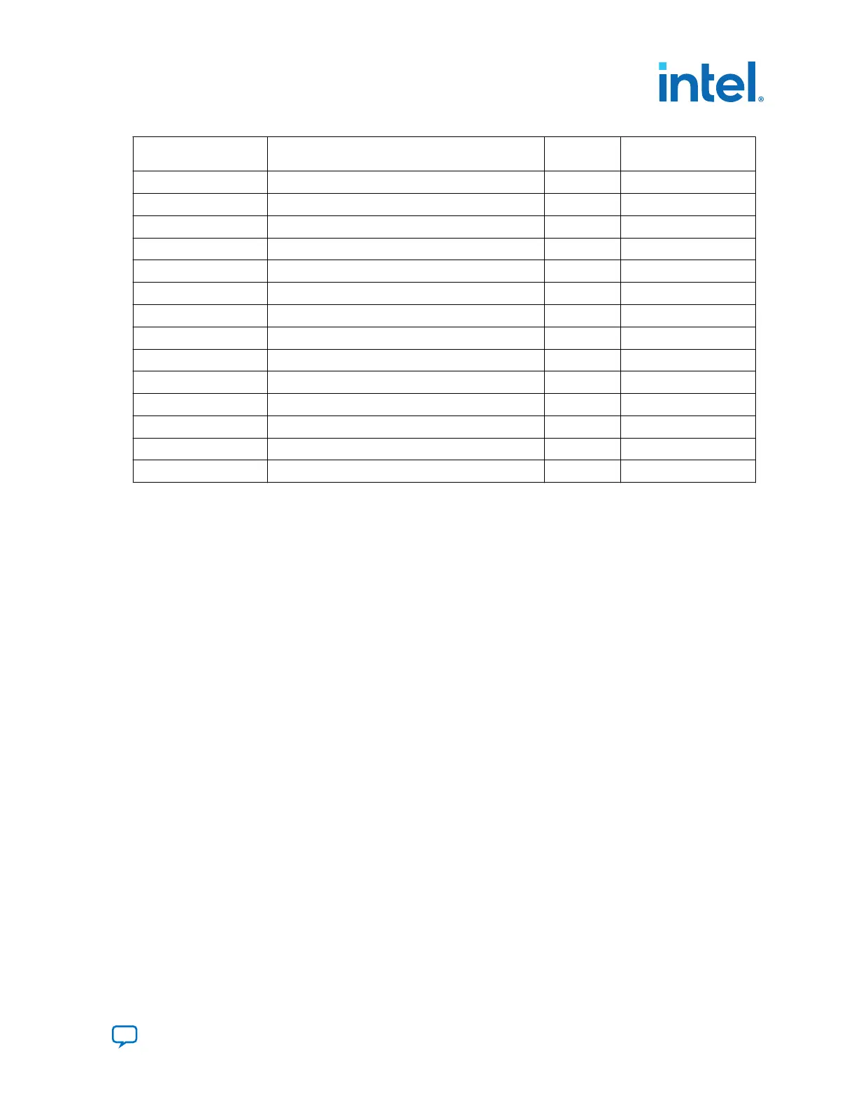
FMCB Connector Pin
Number
Schematic Signal Name FPGA Pin
Number
I/O Standard
D23 FMCB_LA_TX_P11 H13 LVDS
H28 FMCB_LA_TX_P12 M13 LVDS
D26 FMCB_LA_TX_P13 M15 LVDS
H31 FMCB_LA_TX_P14 K20 LVDS
H34 FMCB_LA_TX_P15 L20 LVDS
H37 FMCB_LA_TX_P16 J22 LVDS
F1 FMCB_M2C_PG — —
H2 FMCB_PRSNTN P17 1.8 V
C30 FMCB_SCL J17 1.8 V
C31 FMCB_SDA J16 1.8 V
J39 VIO_B_M2C — —
K40 VIO_B_M2C — —
K1 VREF_B_M2C — —
H1 VREF_FMCB — —
Note: The FMC port B has the same pin assignments as port A but on a different board
reference designation. For example, the pin assignments for FMCA_LA_TX_P1 is
J1.H10 and FMCB_LA_TX_P1 is J2.H10.
6. Board Components
683526 | 2023.07.12
Send Feedback
Intel
®
Arria
®
10 FPGA Development Kit User Guide
97
 Loading...


