VRA53801-R.3609.A
- M4 ・ -
LS-50
Mechanism
1. Hardware
1.1 Body unit
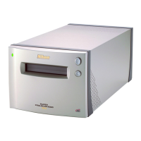
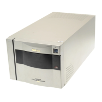
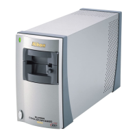
In appearance, the case consists of colored-steel top cover and under-panel, steel plate rear panel,
and plastic front panel. Rubber foot is xed in place on the top cover.
The front panel has the status-indicated LED unit, power switch, and adapter slot.
The rear panel has USB2.0-based interface connector and AC inlets.
Inside the body, a steel-made chassis is framed covering the mechanical unit, main PCB, and power-
supply unit.
1.2 Mechanical unit
The optical scanning system is provided, which consists of illumination optics, projection optics,
and CCD unit. To perform AF, the AF motor (stepping motor) drives the cam, via the reduction
gear, and the mechanical block unit makes up-and-down (near-vertical) movements against the lm.
To perform sub-scanning, by combining the scan motor (stepping motor) and the lead screw, the
mechanical block unit makes right-and-left (near-horizontal) movements against the lm.
1.3 Main PCB (MAIN printed circuit board unit)
The main PC can be divided into MCU unit, custom IC unit, IF (Interface) unit, analog signal
processing unit, illumination LED driving unit, and motor driving unit, according to function.
・MCU unit:
This consists of 16-bit MCU, SS-assembly (Flash memory), 128 KB × 8-bit SRAM × 1, and
RESET IC, etc, and controls entire system (including adapters).
・Custom IC unit:
This performs at 100MHz of the maximum operating frequency. Main functions are image data
scanning, illumination LED lighting-control, DMA control with the host interface, control signal
generation, etc of the CCD and A/D, etc. This also controls input/output with other peripheral
circuitry.
As coefcient memory and line buffer, 32 KB × 8-bit SRAM × 2 and 128 KB ×8-bit SRAM × 2
are connected externally.
・IF unit:
This consists of USB 2.0 controller and USB 2.0 connector.
・Analog signal processing unit:
CCD signal is processed by analog 1 chip IC, which consists of CDS circuit, gain circuit, black
level adjustment circuit, and A/D conversion, then is output to the custom IC.
Gain circuit: 2-level switch
Black level adjustment circuit: The black-level electric potential is adjusted by 8-bit D/A.
A/D conversion circuit: Resolution 14 bits; conversion frequency: 2.778 MHz