Nokia Customer Care TF5 Technical Information
Company Confidential TFE-4/RV-1
Issue 2.0 Mar/2005 Copyright © 2005 Nokia Corporation. Page 8a-3
Company Confidential
List of Figures
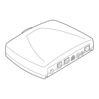
Figure 1: View of TFE-4/RV-1 Radio Unit ..................................................................... 8
Figure 2: Block diagram of the Junctionboard ............................................................. 9
Figure 3: Powerstates of the TFE-4/RV-1 RU ................................................................ 10
Figure 4: Block diagram of Power supply block ........................................................... 12
Figure 5: Vwake Power supply ...................................................................................... 14
Figure 6: VMIC switch a) VMICONX driven low by B2BHFMUTEX ............................... 14
Figure 7: VMIC switch b) VMICONX driven low by B2BHDMOTEX ............................... 14
Figure 8: HW-Realization of Vcar switch ....................................................................... 15
Figure 9: VAudio HW-Realization ................................................................................ 16
Figure 10: VEBpwr regulator HW-Realization ........................................................... 16
Figure 11: VIDDU switch HW-Realization .................................................................... 17
Figure 12: Block diagram of Power control/Reset block ............................................... 18
Figure 13: Vcar Check Realization ................................................................................ 20
Figure 14: SMPS startup realization ..................................................................................... 20
Figure 15: Poweronx realization ................................................................................... 21
Figure 16: IGNS Levelshifter realization ......................................................................... 22
Figure 17: BSI switch .................................................................................................... 22
Figure 18: Block diagram of Audio Block ..................................................................... 22
Figure 19: Realization of HFMIC (Part 1) ..................................................................... 24
Figure 20: Realization of HFMIC (Part 2) ..................................................................... 25
Figure 21: Handsfree Speaker Amplifier Realization .................................................... 25
Figure 22: VNIAS Regulator .......................................................................................... 25
Figure 23: HF-Mute Levelshifter ................................................................................... 26
Figure 24: HD-Power amplifier realization .................................................................... 26
Figure 25: HDMute Levelshifter Realization ................................................................. 27
Figure 26: B2BXEAR filter ............................................................................................. 27
Figure 27: Block diagram of Levelshifter Block ............................................................ 27
Figure 28: CRM Realization .......................................................................................... 28
Figure 29: Realization of the Antenna Line .................................................................. 29
Figure 30: B2B power connectors ................................................................................ 29
Figure 31: B2B system connector ................................................................................. 30
Figure 32: Input Device (ID) connector ......................................................................... 31
Figure 33: Display unit connector ................................................................................ 31
Figure 34: Vcar connector ............................................................................................ 32
Description Page No.
 Loading...