Nokia Customer Care TF4 Technical Information
Company Confidential TFE-4/RV-1
Issue 2.0 Mar/2005 Copyright © 2005 Nokia Corporation. Page 8b-17
Company Confidential
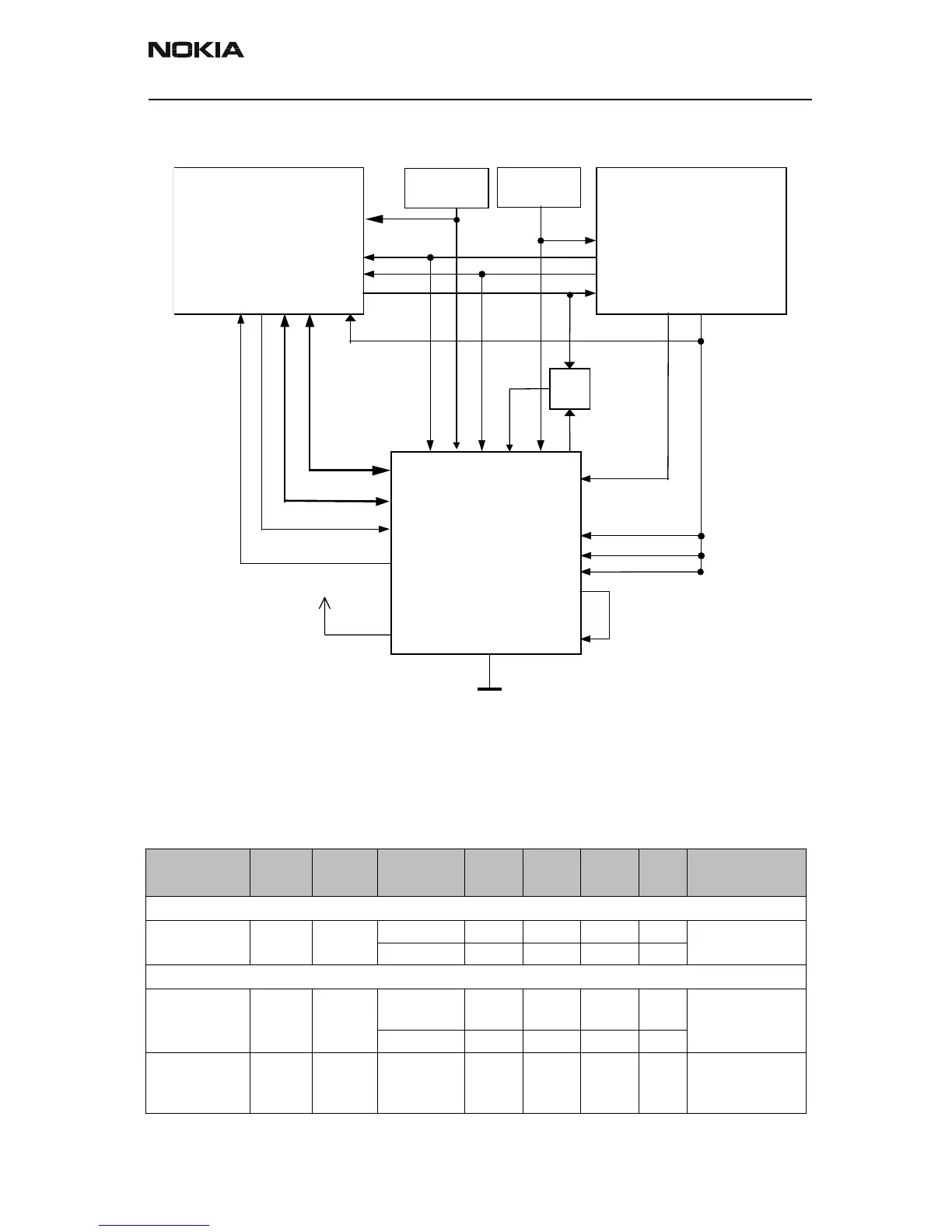
BT-HW interface
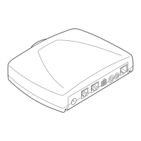
Figure 7: BT102 HW interface
The following table describes the signals covering the interface between the BT module
and the engine. The signal names are referring to the NPL-1 schematic diagram.
Table 2: BT – BB interface description
Signal name
MCM pin #
From To Para-
meter
Min. Typ. Max. Unit Notes
RESET
RESETX
44
UEM
PURX
MCM Logic "1" 1.40 1.80 V BB reset
Logic "0" 0 0.20 V
Clock input
SYSCLCK
50
RF MCM Signal
amplitude
0.30 0.80 Vpp System clock
input
Frequency 26 MHz
EN26MHZ
18
UEM
Vio
MCM Voltage 1.40 1.80 V Defines system
clock. "1" = 26
MHz
HELGE
GPP7 –
FBUS-RX
GPP6 – FBUS-TX
GPP0 - LPRFSync
GPP1 - LPRFIntReq
UPP UEM
VAPPL
VIO
LPRFInt
LPRFSync
USARTRx
USARTTx
SLEEPX
RESETX
SleepClk
SleepClk
Mjölner
RFClk
SYSCLK
Power
Connector
VCC
PURX
PURX
SLPCLK
VBat
VDD
VBBEN
EN26MHZ
GND
 Loading...