Nokia Customer Care TF4 Technical Information
Company Confidential TFE-4/RV-1
Issue 2.0 Mar/2005 Copyright © 2005 Nokia Corporation. Page 8b-47
Company Confidential
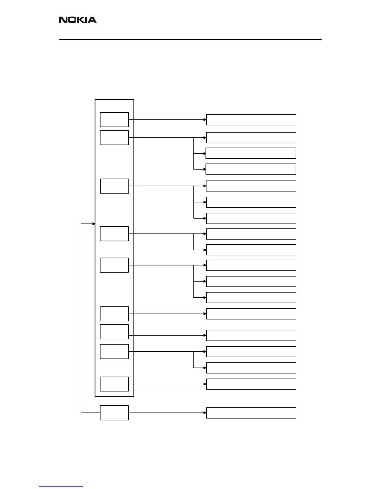
RF Power Supply Configuration
All power supplies for the RF Unit are generated in the UEM IC (D200). All RF supplies
can be checked either in Mjoelner can or in BB can. The power supply configuration used
is shown in the block diagram below. Values of voltages are given as nominal outputs of
UEM. Currents are typical values.
Figure 33: RF Power distribution diagram
VR1A
4.75 V 3.2 %
charge pump (VDDCP)
0.45 mA
85 mA
Tx modulator (VDDTX)
2.78 V 3 %
4.4 mA
2.78 V 3 %
VCXO (VDDXO)
BB buffer (VDDBBB)
BT buffer
14 mA (Tx900), 28 (Rx)
2.78 V 3 %
VR4
VR3
VR2
41 mA
PLL prescaler (VDDPRE)
2.78 V 3 %
VR5
PLL counters (VDDPLL)
dividers, LO buffers (VDDLO)
11 mA
Rx front end (VDDRXF)
2.78 V 3 %
VR6
Rx BB section (VDDRXBB)
14 mA
external VCO
2.78 V 3 %
VR7
0.02 mA
13/26 MHz (SELADDR)
1.8 V 4.5 %
VIO
UEM
Triple band PA, Bluetooth
VBAT
3.6 V
dig. interface (VDDDL)
100 uA
bias reference (VBEXT)
1.35 V 2 %
VREF01
Dig. control (VDDDIG)
Ant. switch control lines
Tx buffer
 Loading...