TFE-4/RV-1 Company Confidential
TF4 Technical Information Nokia Customer Care
Page 8b-6 Copyright © 2005 Nokia Corporation. Issue 2.0 Mar/2005
Company Confidential
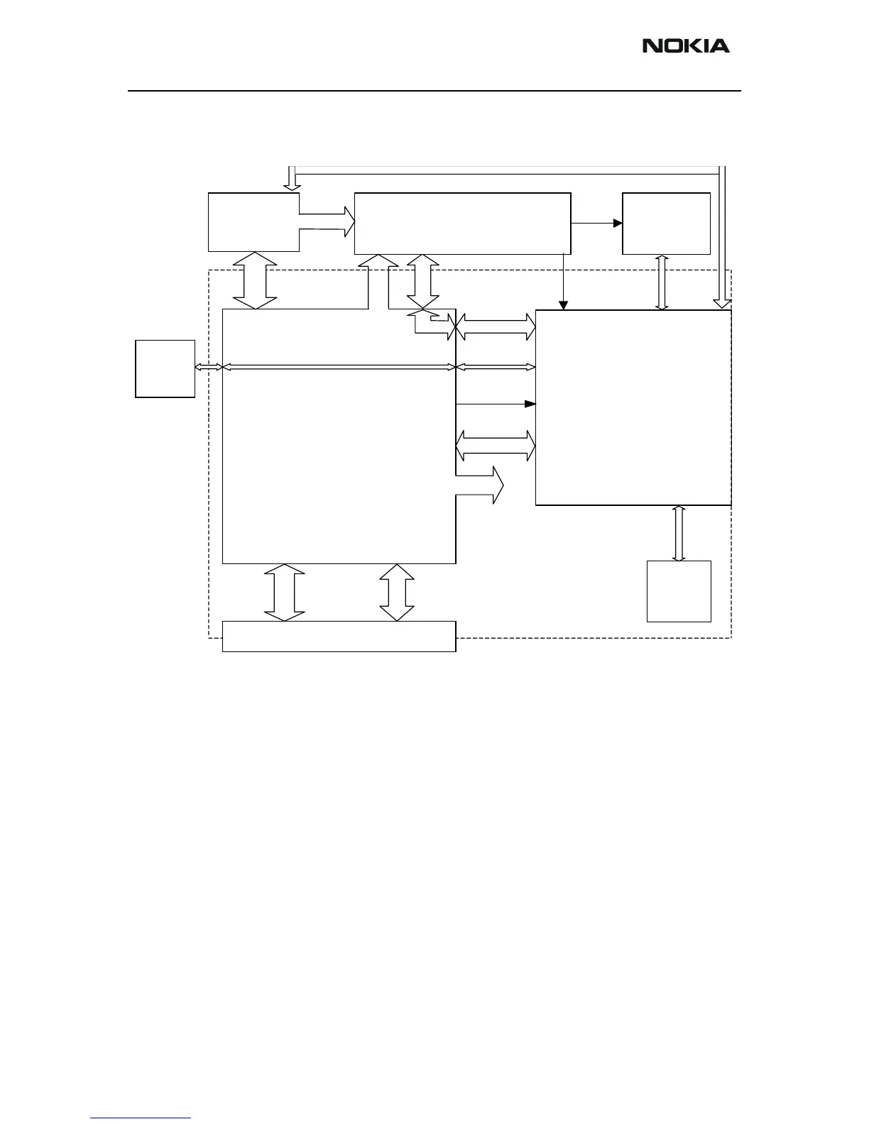
Block diagram of Engine Board
Figure 1: Block Diagram of the Engine Board
A block diagram is shown in Figure 1. The baseband module contains 2 Asics namely the
Universal Energy Management (UEM) and the Universal Phone Processor (UPP). The
baseband module furthermore contains the Bluetooth module. The baseband is based on
the DCT4 engine program.
The UEM supplies both the baseband module as well as the RF module with a series of
voltage regulators. The RF module is supplied with regulated voltages 4.75 V and 2.78 V
and the baseband module with 2.78 V and 1.80 V. The UEM is furthermore supplying the
baseband SIM interface with a programmable voltage of either 1.8 V or 3.0 V and the
core of the UPP is supplied with a programmable voltage of 1.0 V, 1.3 V, 1.5 V or 1.8 V.
The UEM contains a series of PWM sourced drivers. The individual PWM signals are gen-
erated internally within the digital part of the UEM and distributed to the drivers.
The UEM contains a real-time clock sliced down from the 32768 Hz crystal oscillator. The
32768 Hz clock is fed to the UPP as a sleep clock.
Clock
26 MHz
UEM
UPP
SIM
FLASH
B2B Power/
RS232-
Connector
CBUS/
DBUS
RF Supplies
B2B System connector
Bluetooth
RF RX/TX
MBus/FBus
Audio
Controllines
CBUS
USART
Clock
26 MHz
SLEEPCLK
32kHz
Baseband
SIMIF
PA Supply
BB
Supplies
RF (Mjölner)
RF RX/TX
RS232
*** Note: RS232 facility is only utilised in the N810 ***
 Loading...