TFE-4/RV-1 Company Confidential
TF4 Technical Information Nokia Customer Care
Page 8b-18 Copyright © 2005 Nokia Corporation. Issue 2.0 Mar/2005
Company Confidential
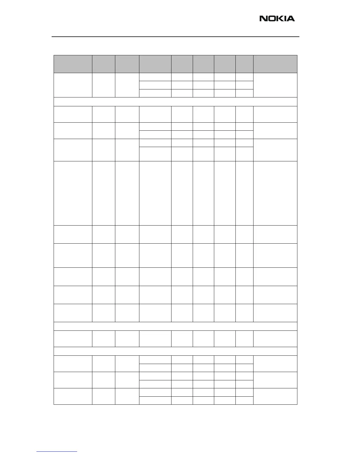
SLPCLK
26
UEM
Sleep-
Clk
MCM Logic "1" 1.26 1.80 V Sleep clock input
Logic "0" 0 0.54 V
Frequency 32763 32768 32773 Hz
Power control
VBBEN
49
UEM
Vio
MCM Voltage 1.40 1.80 V Stan2 regulators
enable
SLEEPX
48
AND
circuit
MCM Logic "1" 1.40 1.80 V Active mode =
"1"
Logic "0" 0 0.20 V
OSCON
31
MCM AND
circuit
Logic "1" 1.40 1.80 V Reflects MCM
status. Active
mode = "1"
Logic "0" 0 0.20 V
GND
1, 2, 3, 4, 5,
6, 7, 8, 9, 10,
11, 16, 17,
13, 14, 15,
19, 24, 29,
33, 39, 43,
47, 51, 56
Voltage 0 V Ground
reference
VCC
52, 53, 54
Vbatt MCM Voltage 2.95 5.20 V Main power
supply input
VREG
6
UEM
Vflash1
MCM Voltage 2.70 2.86 V Regulated
power supply
input
VDD
45
MCM MCM
VPP
Voltage 1.80 V Supply for VPP
VPP
41
MCM
VDD
MCM Voltage 1.80 V Programming
voltage supply
VAPPL
32
UEM
Vio
MCM Voltage 1.80 V Supply for
application IF
RF air
ANT
12
MCM BT ant. Impedance 50
Ω
Antenna pin
General purpose I/O
GPP0
38
MCM LPRF
Sync
Logic "1" 1.26 1.80 V
Logic "0" 0 0.54 V
GPP1
37
MCM LPRF
Int
Logic "1" 1.26 1.80 V
Logic "0" 0 0.54 V
GPP6
28
MCM USART
Rx
Logic "1" 1.26 1.80 V
Logic "0" 0 0.54 V
Table 2: BT – BB interface description
Signal name
MCM pin #
From To Para-
meter
Min. Typ. Max. Unit Notes
 Loading...