Nokia Customer Care TF4 Technical Information
Company Confidential TFE-4/RV-1
Issue 2.0 Mar/2005 Copyright © 2005 Nokia Corporation. Page 8b-25
Company Confidential
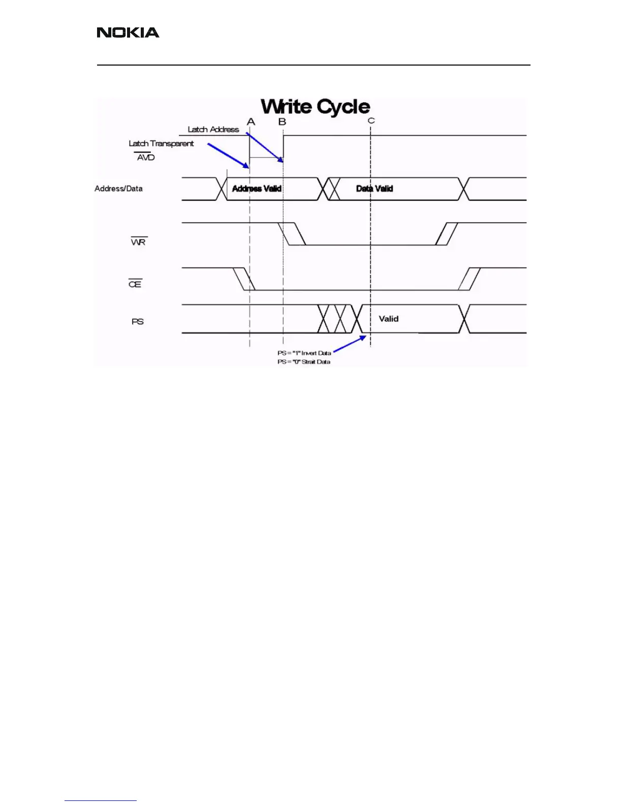
Figure 11: Write Cycle to Flash
Power saving signal (PS).
In order to reduce the power consumption on the bus a Power Save function is intro-
duced. This function reduces the amount of switching on the external bus. Power is con-
sumed in a digital system when a signal changes state. The power is consumed when the
capacitive load is either charged or discharged. The capacitive load is introduced by the
interconnection itself and of cause by the input at the receiving device. Internally in dig-
ital circuits the capacitive load is lower, than at the interconnect level at the printed cir-
cuit board. Therefore it is an advantage if the amount of changes on the external
interconnection, i.e. between two digital circuits, can be minimized. Therefore on a wide
bus like an address/data bus in a microprocessor system, power is saved, if the data to be
transmitted on the external bus, causes a minimum amount of transitions. This can be
achieved by comparing the previously data on the bus, with the data to be transmitted,
and if inverting the data to be transmitted causes less transitions to be performed on the
external bus, the data is inverted, before it is output on the data bus. To inform that the
data is inverted, a control signal is used to inform the receiving device, that the data
must be inverted before any further processing. Data on the address/data bus is bit wise
compared which means that the data previously on D0 (D0e) is compared with the new
data to be output on D0 (D0i). If the two data elements are the same (D0e=D0i) a logic
“0” is indicated to the comparing device. If the two data elements are not the same
(D0e=NOT(D0i)) a logic “1” is indicated to the comparing device. If there are more equal
signal than unequal signals on the address/data bus, the new data is not inverted before
it is sent out on the bus. If there are more unequal than equal data on the address/data
bus, the data is inverted before it is sent out on the bus. The status whether the data that
is presented on the address/data bus is inverted or not, is indicated by a separate signal

 Loading...