Parker Hannifin
P Series User Guide 6
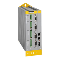
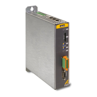
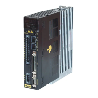
Figure 3. 1000W Drive Front Description ......................................................................................... 19
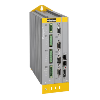
Figure 4. 3500W Drive Front Description ......................................................................................... 19
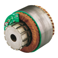
Figure 5. PM Motor Names ................................................................................................................ 20
Figure 6. PD Drive Dimensions ......................................................................................................... 24
Figure 7. PM-FAL series Motor Dimension ....................................................................................... 25
Figure 8. PM-FBL series Motor Dimension ....................................................................................... 26
Figure 9. PM-FCL series Motor Dimension ...................................................................................... 27
Figure 10. PM-FE series Motor Dimension ....................................................................................... 28
Figure 11. PM-FF series Motor Dimension ....................................................................................... 29
Figure 12. PD-04P Mounting Information ......................................................................................... 31
Figure 13. PD-10P Mounting Information ......................................................................................... 31
Figure 14. PD-35P Mounting Information ......................................................................................... 32
Figure 15. System Installation Overview ............................................................................................ 36
Figure 16. Dynamic Brake Sequence ................................................................................................. 39
Figure 17. PD Drive Block Diagram ................................................................................................. 50
Figure 18. Drive Wiring Example ...................................................................................................... 51
Figure 19. I/O Signal Wiring .............................................................................................................. 59
Figure 20. Example of Digital Input Signal Wiring............................................................................ 60
Figure 21. Example of Digital Output Signal Wiring ......................................................................... 61
Figure 22. Example of Analog Input Signal Wiring ........................................................................... 61
Figure 23. Example of Analog Output Signal Wiring ......................................................................... 62
Figure 24. Example of Pulse Heat Signal Wiring ............................................................................... 62
Figure 25. Example of Open Collector Pulse Input Signal Wiring ................................................... 63
Figure 26. Example of NPN Open Collector Pulse Command Wiring ............................................... 63
Figure 27. RS-422 Multi-Drop Connection Example ......................................................................... 65
Figure 28. Allocating Digital Input Signals ....................................................................................... 96
Figure 29. Allocating Digital Output Signals ................................................................................... 100
Figure 30. Commanded Position ...................................................................................................... 108
Figure 31. Position Response Types ................................................................................................. 110
Figure 32. Control Loop Block Diagram ......................................................................................... 111
Figure 33. Vibration Control ............................................................................................................ 116
Figure 34. Meaning of Notch Filter ................................................................................................. 117
Figure 35. Adaptive Filter Diagram ................................................................................................ 118
Figure 36. Analog Monitor ............................................................................................................... 119
 Loading...