Chapter 3 Functional Description 3-5
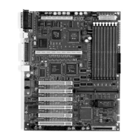
3.3 SPARCengine Ultra AXi Motherboard
The motherboard implementation details appear in the Block Diagram and the
Layout Diagram. It is Fabricated on an 8 layer printed circuit board. Sockets are
provided for the CPU module and the memory DIMMs. The motherboard can be
equipped with a variety of CPU modules (see TABLE 2-1 on page 2-2). Memory
modules are installed in Pairs (two DIMMs at a time) which allow the system to be
equipped with 32MB up to 1GB of memory. There are six 32-bit PCI slots available.
User configurable jumpers are described in A.1 on page A-3.
3.3.1 CPU Module
The UltraSPARC AXi module is a highly integrated CPU with memory controller
and PCI interfaces. The module also includes level-2 cache and high-speed UPA64S
interface for Fast Frame Buffer video module (FFB2). There are five versions of CPU
available at this time: UltraSPARC IIi-270, UltraSPARC IIi-300, UltraSPARC IIi-333,
UltraSPARC IIi-360, UltraSPARC IIi-360R, and UltraSPARC-IIi-440R. The architecture
complies with SPARC V9 instruction set, which enables the system to use a wide
range of peripherals and high performance Solaris 2.6. For further details on the
CPU refer to SME1040 Highly Integrated 64-bit RISC Processor, PCI Interface Data
Sheet document number 805-0086-02.
3.3.2 Main Memory Modules
The Ultra AXi architecture uses 128 data bits + 16 ECC bits in a single memory
access. This is achieved by populating 2 memory DIMMs in a Pair. The Ultra AXi
uses DRAM, EDO, Buffered, 10 or 11-bit Column Address, 3.3V, 60ns, 72-bit, 168-pin
DIMMs. The design has 4 DIMM Pairs of 8 sockets. The 144-bit Memory Data bus is
routed and multiplexed through BMX devices into the CPU Module as a 72-bit bus.
The memory design includes Error Check and Correction (ECC). A single bit error in
a 64-bit word is corrected on the fly. Errors of 2-bits or more are detected and flagged
to system software for error handling. This assures very high data integrity and a
reliable system. The design accommodates different capacity memory modules in 4
Pairs (both DIMMs in a Pair must be the same size). Depending upon the
combination of DIMMs used, it is possible to have from 32MB to 1GB populated.
(32MB, 48MB, 64MB, 80MB, 96MB, 112MB, 128MB...up to 1GB in 16MB increments).
CAS before RAS refresh is used. The memory organization of 10-bit column address
is supported in all DIMM Pairs. 11-bit column address is supported in DIMM Pairs 0
and 2 only. See FIGURE C-14 on page C-17, TABLE C-4 on page C-18 and TABLE C-5
on page C-20 for specific DIMM combinations.