1 2 3 4 5 6 7 8
1 2 3 4 5 6 7 8
A
B
C
DD
C
B
A
Datum
Machine: Title:
SheetDate:
Drawn by: File:
Size:
Änderung NameRev.
J. Wanning
1 1A2 15.09.1995
MA6/BA6
Eingangskarte
103225R03.sch
of
IC1
RN12
8x10k
RN15
8x10k
D1 D2 D3 D4 D5 D6 D7 D8
IC4
1
2
3
4
5
6
7
8
9
11
12
13
14
15
16
17
18
1
2
3
4
5
6
7
8
9
10
11
12
13
14
15
16
17
18
19
T1
2N2222
R2
4k7
R1
15k
GND
+5V
CN1
8x10n
GND
1
2 3 4 5 6 7 8 9
1
2
3
4
5
6
7
89
10
11
12
13
14
15
16
1
23456789
RN1
4x180
RN2
4x180
RN3
4x180
RN4
4x180
RN5
4x180
RN6
4x180
RN7
4x180
RN8
4x180
D9 D10 D11 D12 D13 D14 D15 D16
D17 D18 D19 D20 D21 D22 D23 D24
RN9
8x4k7
1
IC2
RN13
8x10k
RN16
8x10k
IC5
1
2
3
4
5
6
7
8
9
11
12
13
14
15
16
17
18
1
2
3
4
5
6
7
8
9
10
11
12
13
14
15
16
17
18
19
CN2
8x10n
GND
1
2 3 4 5 6 7 8 9
1
2
3
4
5
6
7
89
10
11
12
13
14
15
16
1
23456789
RN10
8x4k7
1
IC3
RN14
8x10k
RN17
8x10k
IC6
1
2
3
4
5
6
7
8
9
11
12
13
14
15
16
17
18
1
2
3
4
5
6
7
8
9
10
11
12
13
14
15
16
17
18
19
CN3
8x10n
GND
1
2 3 4 5 6 7 8 9
1
2
3
4
5
6
7
89
10
11
12
13
14
15
16
1
23456789
RN11
8x4k7
1
IC7
2 3 4 5 6 7 8 9
2 3 4 5 6 7 8 9
2 3 4 5 6 7 8 9
1
2345
1
2345
1
2345
1
2345
1
2345
1
2345
1
2345
1
2345
+5V
GND
GND
GND
GND
GND
GND
GND GND
1 2 3 4 56789101112 13 14 15 16 17 18 19 20 21 22 23 24 25 26 27 28 29 30 31 32
1 2 3 4 56789101112 13 14 15 16 17 18 19 20 21 22 23 24 25 26 27 28 29 30 31 32
1 2 3 4 56789101112 13 14 15 16 17 18 19 20 21 22 23 24 25 26 27 28 29 30 31 32
+24V
C1
47u/35V
+5V
C2
22u/40V
a
b
c
+5V
+5V
+5V
+5V
+5V
+5V
+5V
+5V
+5V
20
20
20
+24V
+24V
+24V
( C5 ) (ALE)
C5
A0
A1
WR
RD
RST
D0
D1
D2
D3
D4
D5
D6
D7
1
2
3
4
5
6
7
8
9
10
11
12
13
14
15
16
17
18
19
20
21
22
23
24
25
+5V
PA0
PA1
PA2
PA3
PA4
PA5
PA6
PA7
PB0
PB1
PB2
PB3
PB4
PB5
PB6
PB7
PC0
PC1
PC2
PC3
PC4
PC5
PC6
PC7
D0
D1
D2
D3
D4
D5
D6
D7
GND
RST
A0
A1
CS
RD
WR
1
2
3
4
5
6
7
8
9
10
11
12
13
14
15
16
17
18
19
20
21
22
23
24
25
27
28
29
30
31
32
33
34
35
36
37
38
39
40
26
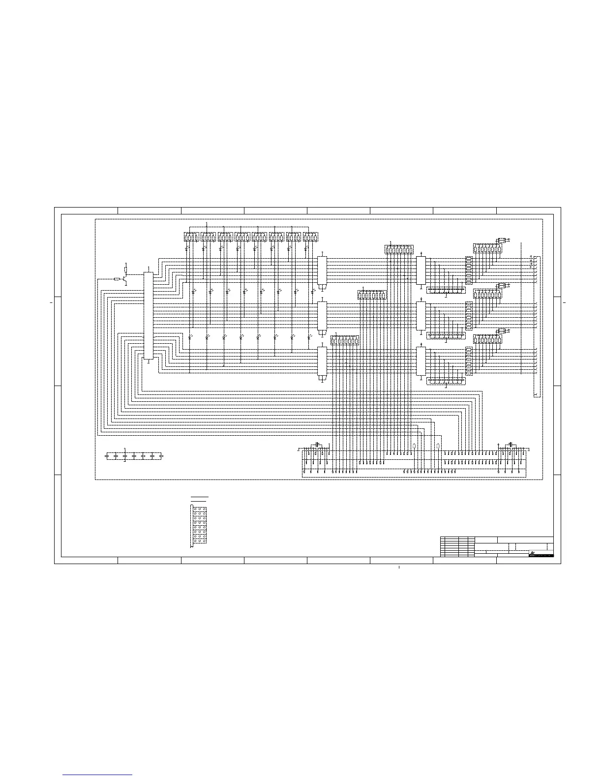
Platine Eingang
PCB input
( 137735 )
S1.1
S1.2
S1.3
S1.4
S1.5
S1.6
S1.7
S1.8
S1.9
S1.10
S9.1
S9.2
S9.3
S9.4
S8.1
S8.2
S8.3
S8.4
S8.5
S8.6
S6.1
S6.3
S6.2
S6.4
SW3.1
SW3.2
SW3.3
SW3.4
S8.7
CV5.1
CV5.2
CV1.1
CV1.2
CV9.7
CV1.3
C2 C3
C3
10n
C4
10n
C5
100n
C6
100n
C7
100n
GND
+5V
Abblockkondensatoren
D1D9D17
D8D16D24
LED-Anordnung :
IC1...IC3 : ULN2803 ( 149642 )
IC4...IC6 : 74LS540 ( 149227 )
IC7 : 8255A ( 149508 )
input card
LED positions :
+24V
+24V
+24V
Anmerkung : Statt der Jumper werden Lötbrücken eingesetzt !
This drawing contains information which
is the proprietary property of Karl Suss.
It is received in confidence and its
contents may not be disclosed without
the prior written consent of Karl Suss.
D1...D24 : LED 3mm grün ( 149643 )
CV1.301 15.09.1995 R. Küster
Rev:
Assy. number:Drawing number:
00103225 113764
Rev:
03
S1.11
S1.12
S.1.13
S1.14
S1.15
Reserve 1
Reserve 2
Reserve 3
Reserve 4
CV9.1 -> CV9.702 06.06.1998 R. Küster
C8
100n
C9
100n
+ C8,903 20.11.00 lge
 Loading...