2AV/X
2-3-14
2-3
2-3-3 CCD PCB
1
2
RS
CLP
SHIFT
Odd
Even
RS
CLP
Logic IC1
Main PCBCCD PCB
Clock signal generator
ASIC
Analog signal
processing circuit
CCD
IC2
Transistor TR2
Transistor TR1
SHIFT
Odd
Even
1
2
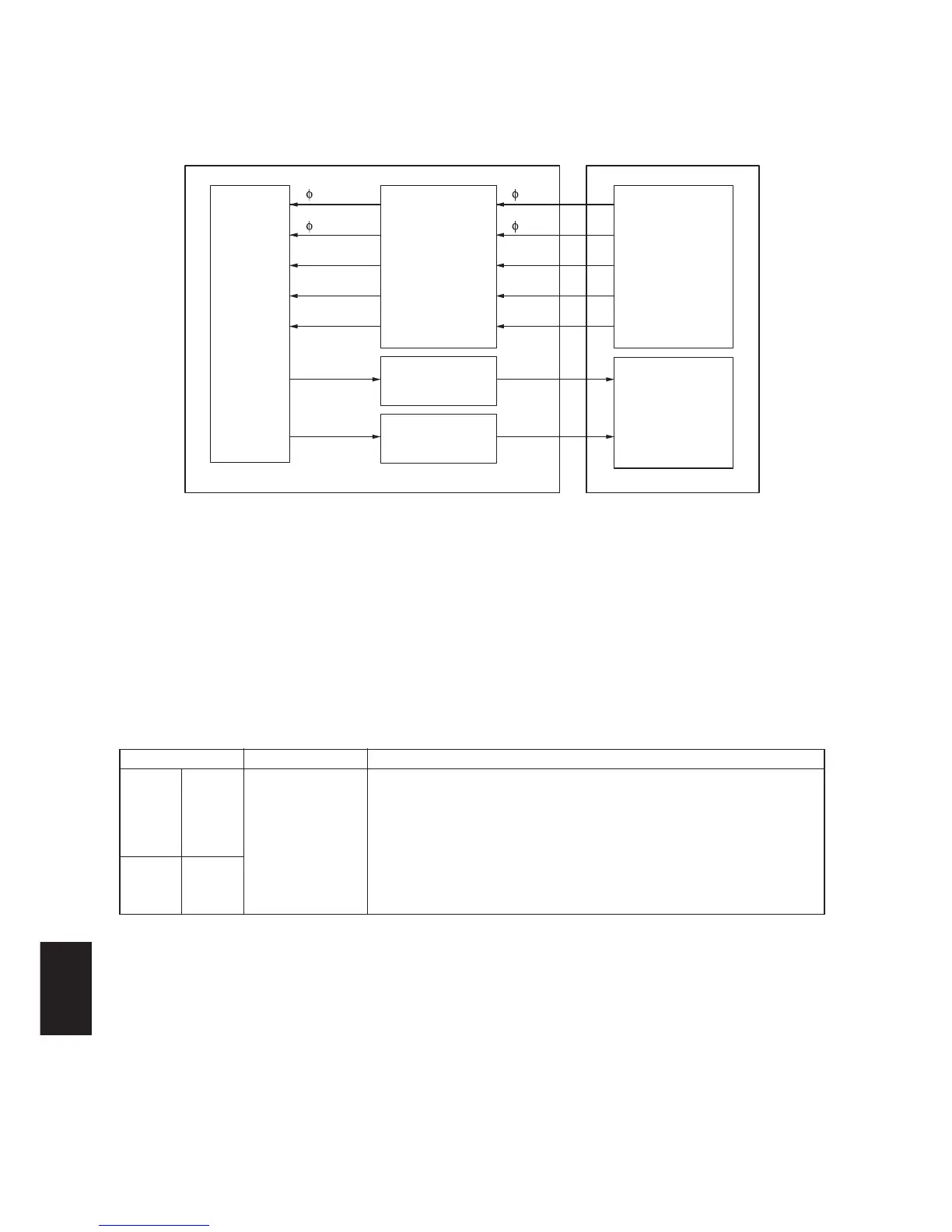
Figure 2-3-7 CCD PCB block diagram
The CCD PCB (CCDPCB) is equipped with a CCD sensor IC2 for original scanning.
The CCD sensor IC2 is controlled by the clock signals φ1, φ2, RS, CLP and SHIFT for CCD drive from the main PCB
(MPCB) via logic IC1.
Image signals are analog signals. Even- and odd-numbered pixels are output separately. These analog image signals are
amplified by emitter followers in the transistors TR1 and TR2 and then transmitted to the analog signal processing circuit in
the main PCB (MPCB).
Terminals (CN) Voltage Remarks
1-1 1-2 0/5 V DC (pulse) CCDPCB clock pulse, input
1-3 1-4 0/5 V DC (pulse) CCDPCB clock pulse, input
1-5 1-6 0/5 V DC (pulse) CCDPCB RESET signal, input
1-7 1-8 0/5 V DC (pulse) CCDPCB CLP signal, input
1-9 1-10 0/5 V DC (pulse) CCDPCB SHIFT signal, input
2-1 2-2 CCDPCB image signal (ODD), output
2-3 2-4 CCDPCB image signal (EVEN), output
2-5 2-6 12 V DC 12 V DC supply from MPCB, input