MicroBlaze Processor Reference Guide 114
UG984 (v2018.2) June 21, 2018 www.xilinx.com
Chapter 2: MicroBlaze Architecture
Profiling Data Read Register
The Profiling Data Read Register (PDRR) reads the bin value indicated by the Profiling Buffer
Address Register and increments the Profiling Buffer Address Register. This register is a read-
only register. Issuing a write request to the register does nothing. See the following figure and
table.
When reading this register with MDM software access to debug registers, data is read with
two consecutive accesses.
Profiling Data Write Register
The Profiling Data Write Register (PDWR) writes a new value to the bin indicated by the
Profiling Buffer Address Register and increments the Profiling Buffer Address Register. This
register is a write-only register. Issuing a read request has no effect, and undefined data is
read.
This register can be used to clear the Profiling Buffer before enabling profiling.
The 4 most significant bits in the Profiling Buffer bin are set to zero when writing the new
value. See the following figure and table.
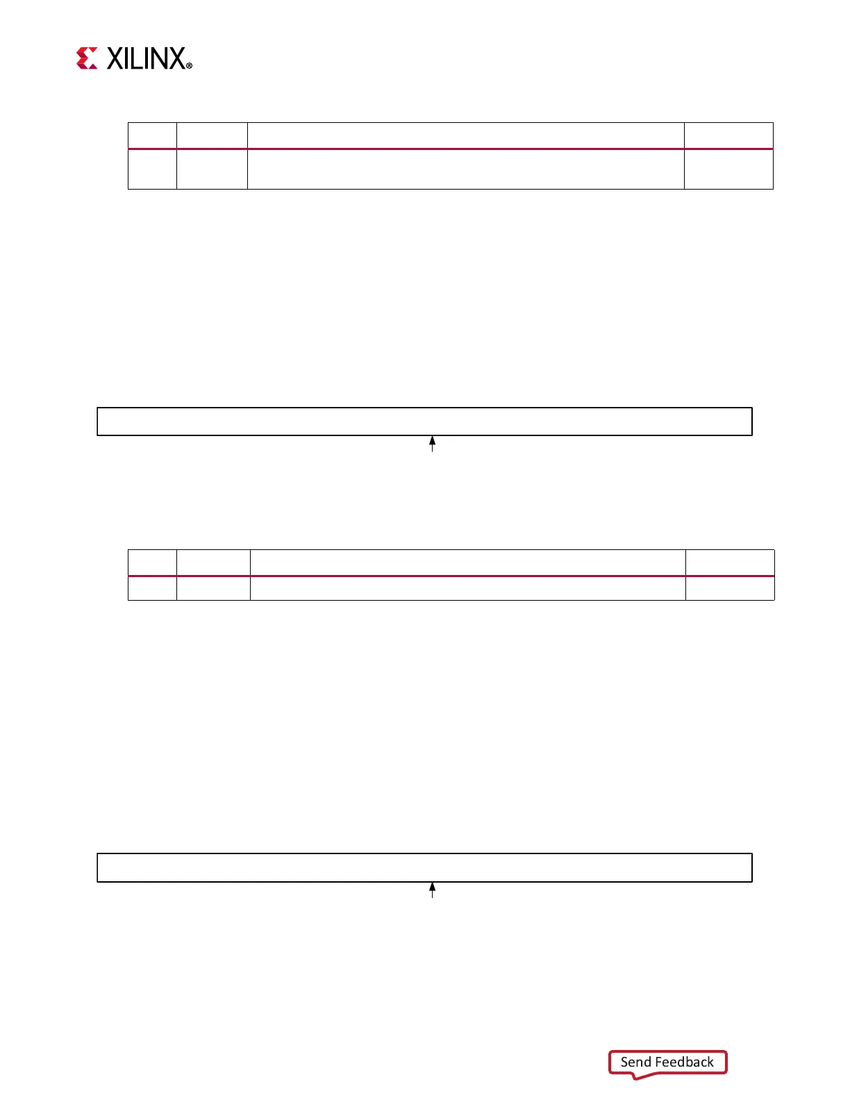
Table 2-59: Profiling Buffer Address Register (PBAR)
Bits Name Description Reset Value
n-1:0 Buffer
Address
Bin in the Profiling Buffer to read or write. The number of bits (n) is 10
for a 4KB buffer, 11 for a 8KB buffer, …, 15 for a 128KB buffer.
0
X-Ref Target - Figure 2-39
Figure 2-39: Profiling Data Read Register
0
Read Data
35
X19775-082517
Table 2-60: Profiling Data Read Register (PDRR)
Bits Name Description Reset Value
35:0 Read Data
Number of executed instructions or executed clock cycles in the bin
0
X-Ref Target - Figure 2-40
Figure 2-40: Profiling Data Write Register
0
Write Data
31
X19776-082517