MicroBlaze Processor Reference Guide 150
UG984 (v2018.2) June 21, 2018 www.xilinx.com
Chapter 3: MicroBlaze Signal Interface Description
cache interface. If the parameter is 0, the cached memory range is accessed over the
AXI4 peripheral interface when the caches are software disabled (that is, MSR[ICE]=0).
• With a 32-bit master, the data cache interface (
M_AXI_DC or M_ACE_DC) performs single
word accesses, as well as 4 word, 8 word or 16 word burst accesses, depending on
cache line length. Burst write accesses are only performed when using write-back cache
with AXI4. With 128-bit, 256-bit, or 512-bit AXI4 masters, only single accesses are
performed.
This interface can have multiple outstanding transactions, either issuing up to 2
transactions when reading, or up to 32 transactions when writing. MicroBlaze ensures
that all outstanding writes are completed before a read is issued, since the processor
must maintain an ordered memory model but AXI4 or ACE has separate read/write
channels without any ordering. Using up to 32 outstanding write transactions improves
performance, since it allows multiple writes to proceed without stalling the pipeline.
Word, halfword and byte writes are performed by setting the appropriate byte strobes.
Exclusive accesses can be enabled for LWX and SWX instructions.
How memory locations are accessed depend on the parameter
C_DCACHE_ALWAYS_USED. If the parameter is 1, the cached memory range is always
accessed using the AXI4 or ACE cache interface. If the parameter is 0, the cached
memory range is accessed over the AXI4 peripheral interface when the caches are
software disabled (that is, MSR[DCE]=0).
Interface Parameters and Signals
The relationship between MicroBlaze parameter settings and AXI4 interface behavior for
tool-assigned parameters is summarized in the following table.
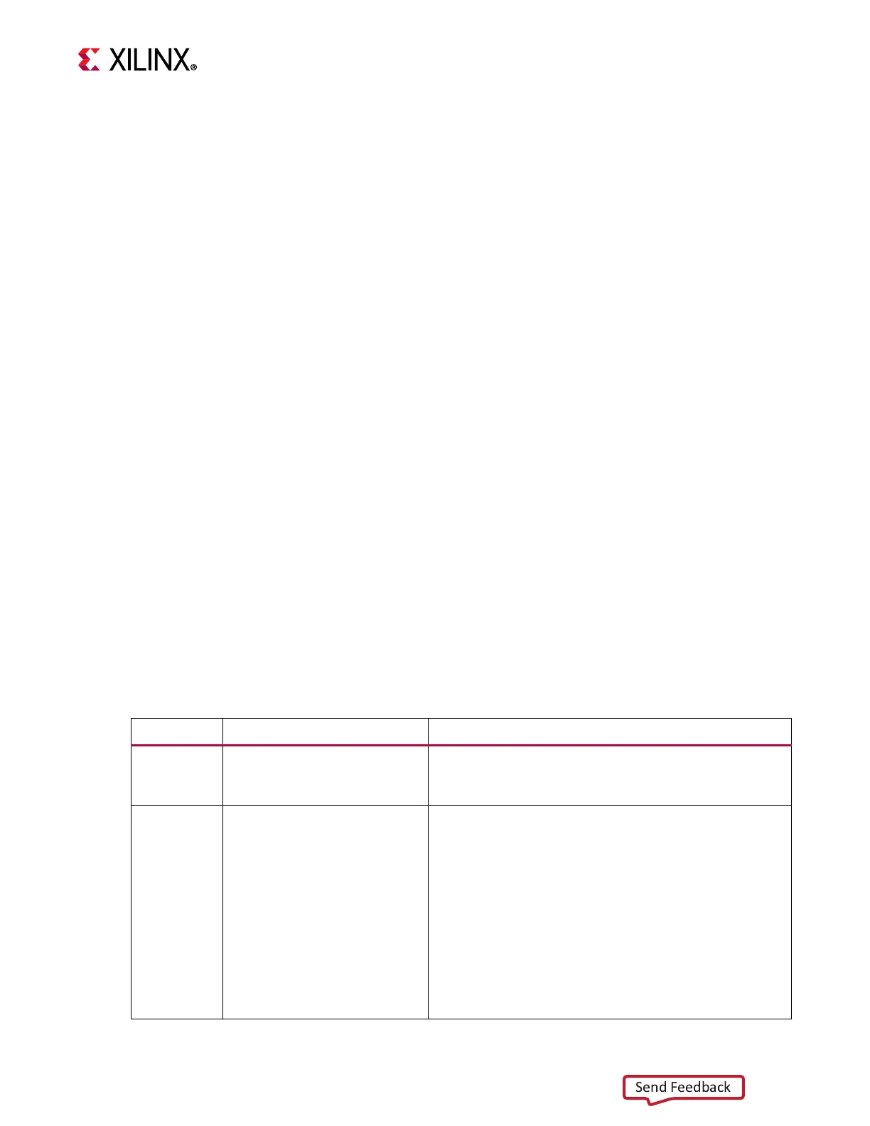
Table 3-5: AXI Memory Mapped Interface Parameters
Interface Parameter Description
M_AXI_DP C_M_AXI_DP_PROTOCOL AXI4-Lite: Default.
AXI4: Used to allow exclusive access when
C_M_AXI_DP_EXCLUSIVE_ACCESS is 1.
M_AXI_IC
M_ACE_IC
C_M_AXI_IC_DATA_WIDTH 32: Default, single word accesses and burst accesses
with C_ICACHE_LINE_LEN word busts used with AXI4
and ACE.
128: Used when C_ICACHE_DATA_WIDTH is set to 1
and C_ICACHE_LINE_LEN is set to 4 with AXI4. Only
single accesses can occur.
256: Used when C_ICACHE_DATA_WIDTH is set to 1
and C_ICACHE_LINE_LEN is set to 8 with AXI4. Only
single accesses can occur.
512: Used when C_ICACHE_DATA_WIDTH is set to 2, or
when it is set to 1 and C_ICACHE_LINE_LEN is set to
16 with AXI4. Only single accesses can occur.