EasyManuals Logo

Xilinx MicroBlaze Reference Guide

Xilinx MicroBlaze
316 pages
To Next Page IconTo Next Page
To Previous Page IconTo Previous Page
Page #157 background imageLoading...
Page #157 background image
MicroBlaze Processor Reference Guide 158
UG984 (v2018.2) June 21, 2018 www.xilinx.com
Chapter 3: MicroBlaze Signal Interface Description
LMB Transactions
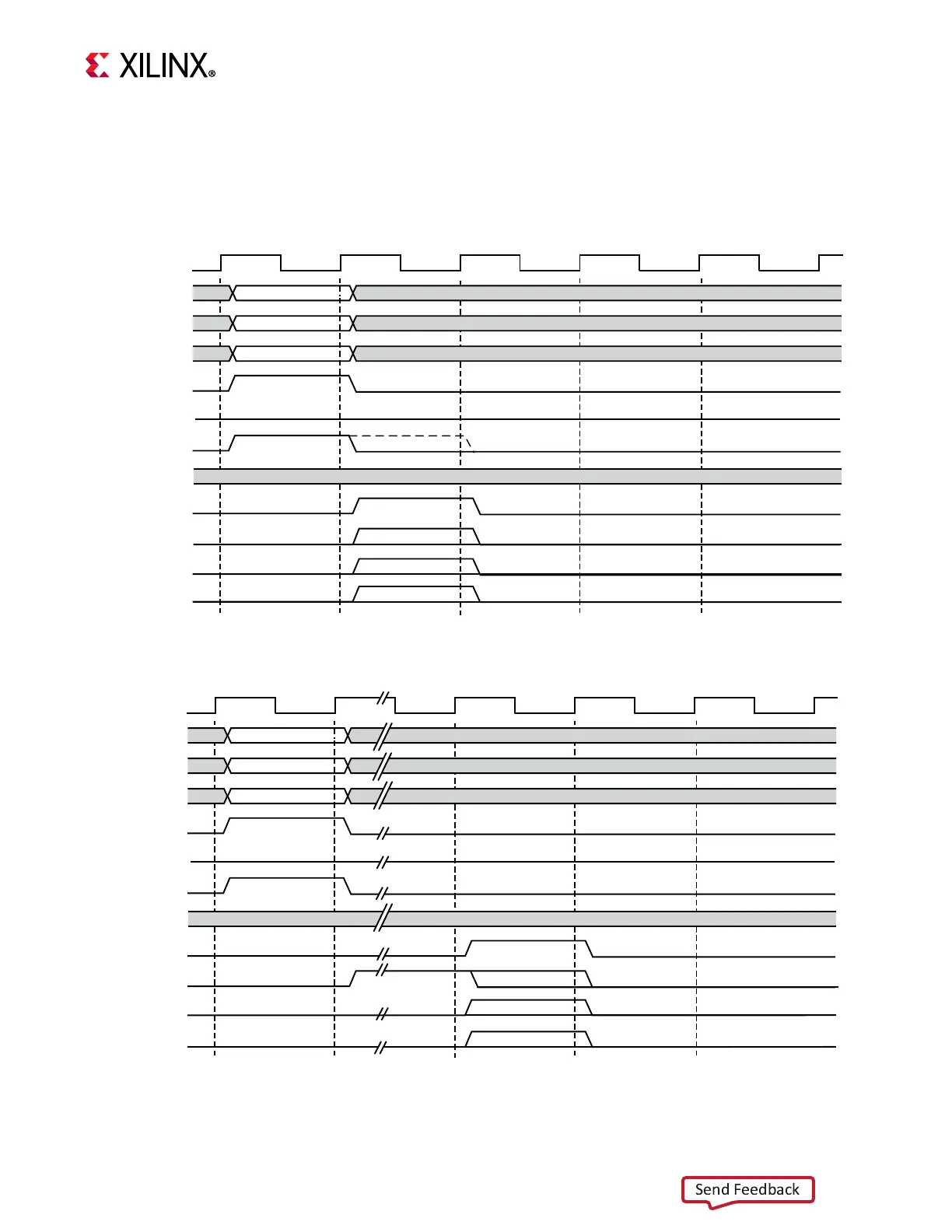
The following diagrams provide examples of LMB bus operations.
Generic Write Operations
X-Ref Target - Figure 3-4
Figure 3-4: LMB Generic Write Operation, 0 Wait States
A0
BE0
D0
Don’t Care
Clk
Addr
Byte_Enable
Data_Write
AS
Read_Strobe
Wirte_Strobe
Data_Read
Ready
Wait
CE
UE
X19788-091217
X-Ref Target - Figure 3-5
Figure 3-5: LMB Generic Write Operation, N Wait State
A0
BE0
D0
Don’t Care
Clk
Addr
Byte_Enable
Data_Write
AS
Read_Strobe
Wirte_Strobe
Data_Read
Ready
Wait
CE
UE
X19789-091217
Send Feedback

Table of Contents

Other manuals for Xilinx MicroBlaze

Questions and Answers:

Question and Answer IconNeed help?

Do you have a question about the Xilinx MicroBlaze and is the answer not in the manual?

Xilinx MicroBlaze Specifications

General IconGeneral
Architecture32-bit RISC
CacheConfigurable Instruction and Data Cache
CategorySoft Processor Core
Data Width32-bit
Memory Management Unit (MMU)Optional
Floating Point Unit (FPU)Optional
Interrupt ControllerConfigurable
Memory ManagementOptional MMU
ConfigurabilityHighly Configurable
Pipeline Stages3-stage
FPGA IntegrationXilinx FPGAs
Bus InterfacePLB
Debug InterfaceJTAG
Typical Clock SpeedVaries depending on FPGA and configuration (e.g., 100-400+ MHz)
ImplementationSoft core (synthesized logic)
Maximum PerformanceVaries with FPGA and configuration
Debug SupportIntegrated Debug Module

Related product manuals