MicroBlaze Processor Reference Guide 163
UG984 (v2018.2) June 21, 2018 www.xilinx.com
Chapter 3: MicroBlaze Signal Interface Description
Note: Other masters could have more restrictive requirements for byte lane placement than those
allowed by MicroBlaze. Slave devices are typically attached “left-justified” with byte devices attached
to the most-significant byte lane, and halfword devices attached to the most significant halfword
lane. The MicroBlaze steering logic fully supports this attachment method.
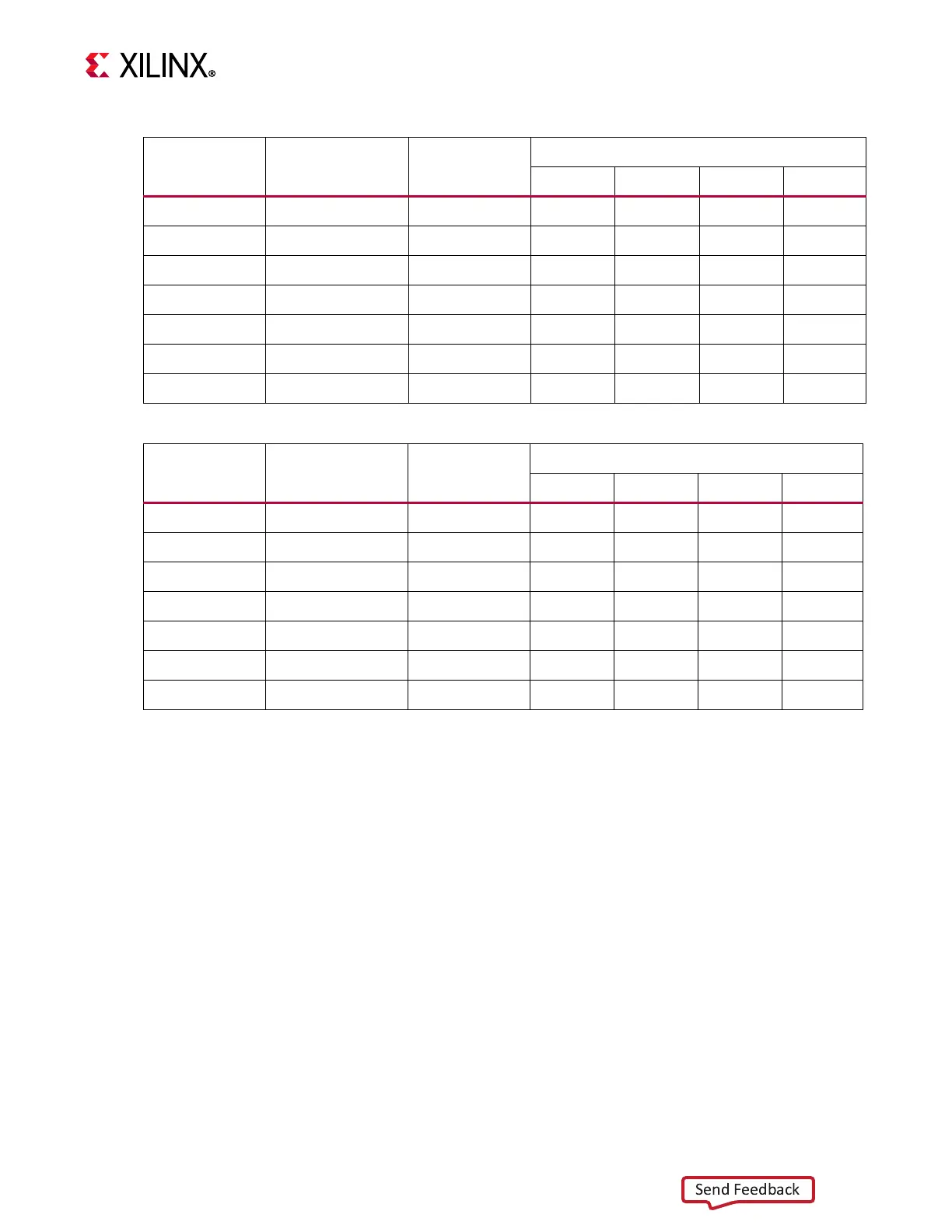
Table 3-11: Big Endian Write Data Steering (Store from Register rD)
Address
[LSB-1:LSB]
Byte_Enable
[0:3]
Transfer Size
Write Data Bus Bytes
Byte0 Byte1 Byte2 Byte3
11 0001 byte
rD[24:31]
10 0010 byte
rD[24:31]
01 0100 byte
rD[24:31]
00 1000 byte
rD[24:31]
10 0011 halfword
rD[16:23] rD[24:31]
00 1100 halfword
rD[16:23] rD[24:31]
00 1111 word
rD[0:7] rD[8:15] rD[16:23] rD[24:31]
Table 3-12: Little Endian Write Data Steering (Store from Register rD)
Address
[LSB-1:LSB]
Byte_Enable
[0:3]
Transfer Size
Write Data Bus Bytes
Byte3 Byte2 Byte1 Byte0
11 1000 byte
rD[24:31]
10 0100 byte
rD[24:31]
01 0010 byte
rD[24:31]
00 0001 byte
rD[24:31]
10 1100 halfword
rD[16:23] rD[24:31]
00 0011 halfword
rD[16:23] rD[24:31]
00 1111 word
rD[0:7] rD[8:15] rD[16:23] rD[24:31]