MicroBlaze Processor Reference Guide 179
UG984 (v2018.2) June 21, 2018 www.xilinx.com
Chapter 3: MicroBlaze Signal Interface Description
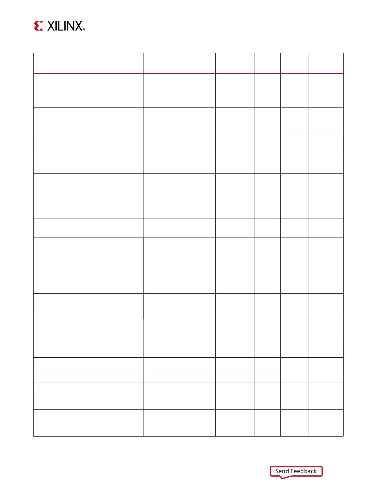
C_ICACHE_ALWAYS_USED Instruction cache
interface used for all
memory accesses in the
cacheable range
0, 1 1
integer
C_ICACHE_FORCE_TAG_LUTRAM Instruction cache tag
always implemented
with distributed RAM
0, 1 0
integer
C_ICACHE_STREAMS Instruction cache
streams
0, 1 0
integer
C_ICACHE_VICTIMS Instruction cache
victims
0, 2, 4, 8 0
integer
C_ICACHE_DATA_WIDTH Instruction cache data
width
0 = 32 bits
1 = Full cache line
2 = 512 bits
0, 1, 2 0
integer
C_ADDR_TAG_BITS Instruction cache
address tags
0-25 17
yes
integer
C_CACHE_BYTE_SIZE Instruction cache size 64, 128,
256, 512,
1024, 2048,
4096, 8192,
16384,
32768,
65536
1
8192
integer
C_DCACHE_BASEADDR Data cache base address
0x0 -
0xFFFFFFFF
FFFFFFFF
0x0
std_logic_
vector
C_DCACHE_HIGHADDR Data cache high address
0x0 -
0xFFFFFFFF
FFFFFFFF
0x3FFFF
FFF
std_logic_
vector
C_USE_DCACHE Data cache 0, 1 0 integer
C_ALLOW_DCACHE_WR Data cache write enable 0, 1 1 integer
C_DCACHE_LINE_LEN Data cache line length 4, 8, 16 4 integer
C_DCACHE_ALWAYS_USED Data cache interface
used for all accesses in
the cacheable range
0, 1 1
integer
C_DCACHE_FORCE_TAG_LUTRAM Data cache tag always
implemented with
distributed RAM
0, 1 0
integer
Table 3-19: Configuration Parameters (Cont’d)
Parameter Name Feature/Description
Allowable
Values
Default
Value
Tool
Assigned
VHDL Type