MicroBlaze Processor Reference Guide 180
UG984 (v2018.2) June 21, 2018 www.xilinx.com
Chapter 3: MicroBlaze Signal Interface Description
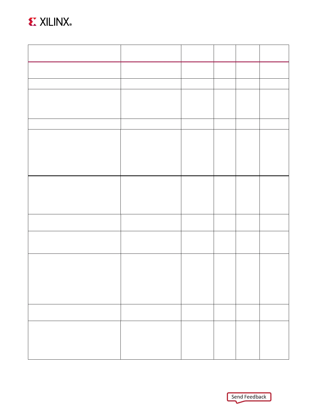
C_DCACHE_USE_WRITEBACK Data cache write-back
storage policy used
0, 1 0
integer
C_DCACHE_VICTIMS Data cache victims 0, 2, 4, 8 0 integer
C_DCACHE_DATA_WIDTH Data cache data width
0 = 32 bits
1 = Full cache line
2 = 512 bits
0, 1, 2 0
integer
C_DCACHE_ADDR_TAG Data cache address tags 0-25 17
yes
integer
C_DCACHE_BYTE_SIZE Data cache size 64, 128,
256, 512,
1024, 2048,
4096, 8192,
16384,
32768,
65536
2
8192
integer
C_USE_MMU
3
Memory Management:
0 = None
1 = User Mode
2 = Protection
3 = Virtual
0, 1, 2, 3 0 integer
C_MMU_DTLB_SIZE
3
Data shadow Translation
Look-Aside Buffer size
1, 2, 4, 8 4 integer
C_MMU_ITLB_SIZE
3
Instruction shadow
Translation Look-Aside
Buffer size
1, 2, 4, 8 2 integer
C_MMU_TLB_ACCESS
3
Access to memory
management special
registers:
0 = Minimal
1 = Read
2 = Write
3 = Full
0, 1, 2, 3 3 integer
C_MMU_ZONES
3
Number of memory
protection zones
0-16 16 integer
C_MMU_PRIVILEGED_INSTR
3
Privileged instructions
0 = Full protection
1 = Allow stream instrs
2 = Allow extended addr
3 = Allow both
0,1,2,3 0 integer
Table 3-19: Configuration Parameters (Cont’d)
Parameter Name Feature/Description
Allowable
Values
Default
Value
Tool
Assigned
VHDL Type