MicroBlaze Processor Reference Guide 18
UG984 (v2018.2) June 21, 2018 www.xilinx.com
Chapter 2: MicroBlaze Architecture
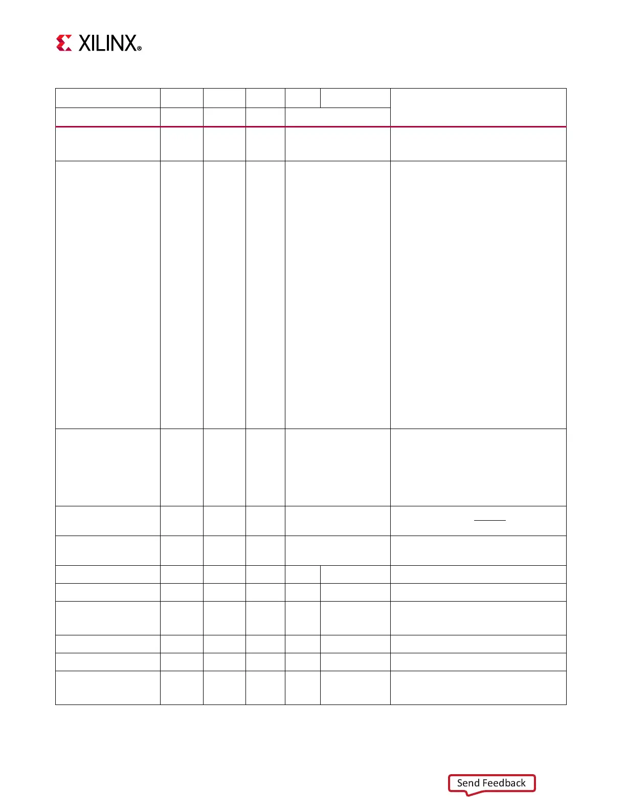
MTSE Sd,Ra 100101 01000 Ra 11 & Sd SPR[Sd} := Ra, where:
· SPR[0x1003] is TLBLO[MSH]
MFS Rd,Sa 100101 Rd 00000 10 & Sa Rd := SPR[Sa], where:
· SPR[0x0000] is PC
· SPR[0x0001] is MSR
· SPR[0x0003] is EAR[LSH]
· SPR[0x0005] is ESR
· SPR[0x0007] is FSR
· SPR[0x000B] is BTR
· SPR[0x000D] is EDR
· SPR[0x0800] is SLR
· SPR[0x0802] is SHR
· SPR[0x1000] is PID
· SPR[0x1001] is ZPR
· SPR[0x1002] is TLBX
· SPR[0x1003] is TLBLO[LSH]
· SPR[0x1004] is TLBHI
· SPR[0x2000-200B] is PVR[0-
12][LSH]
MFSE Rd,Sa 100101 Rd 01000 10 & Sa Rd := SPR[Sa][MSH], where:
· SPR[0x0003] is EAR[MSH]
· SPR[0x1003] is TLBLO[MSH]
· SPR[0x2006-2009] is PVR[6-
9][MSH]
MSRCLR Rd,Imm 100101 Rd 00001 00 & Imm14 Rd := MSR
MSR := MSR and Imm14
MSRSET Rd,Imm 100101 Rd 00000 00 & Imm14 Rd := MSR
MSR := MSR or Imm14
BR Rb 100110 00000 00000 Rb 00000000000 PC := PC + Rb
BRD Rb 100110 00000 10000 Rb 00000000000 PC := PC + Rb
BRLD Rd,Rb 100110 Rd 10100 Rb 00000000000 PC := PC + Rb
Rd := PC
BRA Rb 100110 00000 01000 Rb 00000000000 PC := Rb
BRAD Rb 100110 00000 11000 Rb 00000000000 PC := Rb
BRALD Rd,Rb 100110 Rd 11100 Rb 00000000000 PC := Rb
Rd := PC
Table 2-6: MicroBlaze Instruction Set Summary (Cont’d)
Type A 0-5 6-10 11-15 16-20 21-31
Semantics
Type B 0-5 6-10 11-15 16-31