MicroBlaze Processor Reference Guide 244
UG984 (v2018.2) June 21, 2018 www.xilinx.com
Chapter 5: MicroBlaze Instruction Set Architecture
lbui
Load Byte Unsigned Immediate
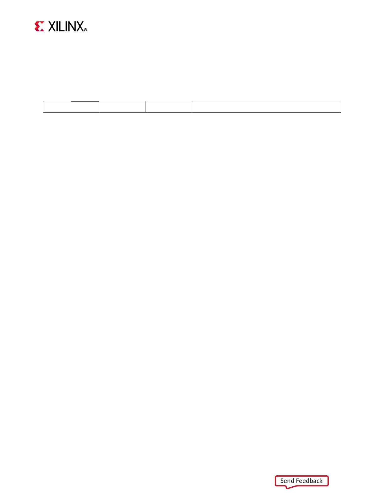
lbui
rD, rA, IMM
1 1 1 0 0 0 rD rA IMM
0 6 11 16
31
Description
Loads a byte (8 bits) from the memory location that results from adding the contents of register rA
with the value in IMM, sign-extended to 32 bits. The data is placed in the least significant byte of
register rD and the other three bytes in rD are cleared.
A data TLB miss exception occurs if virtual protected mode is enabled, and a valid translation entry
corresponding to the address is not found in the TLB.
A data storage exception occurs if access is prevented by a no-access-allowed zone protection. This
only applies to accesses with user mode and virtual protected mode enabled.
Pseudocode
Addr ← (rA) + sext(IMM)
if TLB_Miss(Addr) and MSR[VM] = 1 then
ESR[EC]
← 10010;ESR[S]← 0
MSR[UMS] ← MSR[UM]; MSR[VMS] ← MSR[VM]; MSR[UM] ← 0; MSR[VM] ← 0
else if Access_Protected(Addr) and MSR[UM] = 1 and MSR[VM] = 1 then
ESR[EC]
← 10000;ESR[S]← 0; ESR[DIZ] ← 1
MSR[UMS] ← MSR[UM]; MSR[VMS] ← MSR[VM]; MSR[UM] ← 0; MSR[VM] ← 0
else
(rD)[24:31]
← Mem(Addr)
(rD)[0:23] ← 0
Registers Altered
• rD, unless an exception is generated, in which case the register is unchanged
• MSR[UM], MSR[VM], MSR[UMS], MSR[VMS], if an exception is generated
• ESR[EC], ESR[S], if an exception is generated
• ESR[DIZ], if a data storage exception is generated
Latency
• 1 cycle with C_AREA_OPTIMIZED=0 or 2
• 2 cycles with
C_AREA_OPTIMIZED=1
Note
By default, Type B Instructions will take the 16-bit IMM field value and sign extend it to 32 bits to use
as the immediate operand. This behavior can be overridden by preceding the Type B instruction with
an imm instruction. See the instruction
“imm” for details on using 32-bit immediate values.