MicroBlaze Processor Reference Guide 31
UG984 (v2018.2) June 21, 2018 www.xilinx.com
Chapter 2: MicroBlaze Architecture
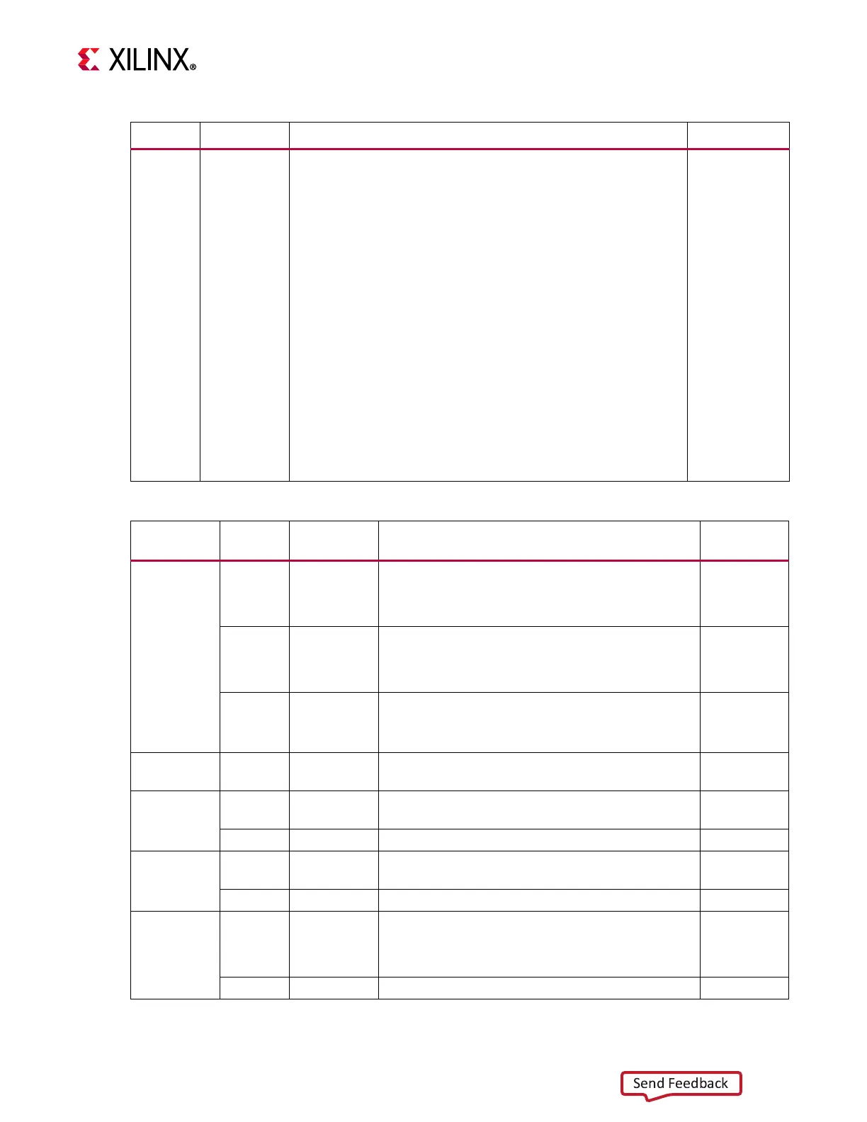
27:31 EC Exception Cause
00000 = Stream exception
00001 = Unaligned data access exception
00010 = Illegal op-code exception
00011 = Instruction bus error exception
00100 = Data bus error exception
00101 = Divide exception
00110 = floating-point unit exception
00111 = Privileged instruction exception
00111 = Stack protection violation exception
10000 = Data storage exception
10001 = Instruction storage exception
10010 = Data TLB miss exception
10011 = Instruction TLB miss exception
Read-only
0
Table 2-12: Exception Specific Status (ESS)
Exception
Cause
Bits Name Description Reset Value
Unaligned
Data Access
20 W Word Access Exception
0 = unaligned halfword access
1 = unaligned word access
0
21 S Store Access Exception
0 = unaligned load access
1 = unaligned store access
0
22:26 Rx Source/Destination Register
General purpose register used as source (Store) or
destination (Load) in unaligned access
0
Illegal
Instruction
20:26 Reserved 0
Instruction
bus error
20 ECC Exception caused by ILMB correctable or
uncorrectable error
0
21:26 Reserved 0
Data bus
error
20 ECC Exception caused by DLMB correctable or
uncorrectable error
0
21:26 Reserved 0
Divide 20 DEC Divide - Division exception cause
0 = Divide-By-Zero
1 = Division Overflow
0
21:26 Reserved 0
Table 2-11: Exception Status Register (ESR) (Cont’d)
Bits Name Description Reset Value