MicroBlaze Processor Reference Guide 46
UG984 (v2018.2) June 21, 2018 www.xilinx.com
Chapter 2: MicroBlaze Architecture
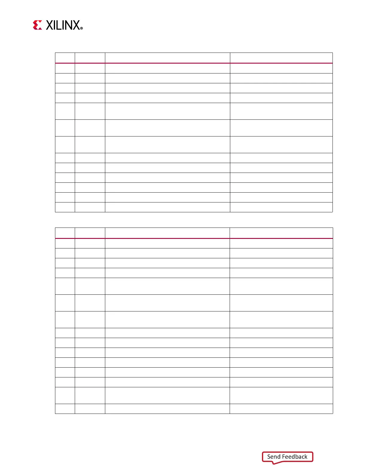
Table 2-28: Processor Version Register 4 (PVR4)
Bits Name Description Value
0 ICU Use instruction cache C_USE_ICACHE
1:5 ICTS Instruction cache tag size C_ADDR_TAG_BITS
6 Reserved 1
7 ICW Allow instruction cache write C_ALLOW_ICACHE_WR
8:10 ICLL The base two logarithm of the instruction
cache line length
log2(C_ICACHE_LINE_LEN)
11:15 ICBS The base two logarithm of the instruction
cache byte size
log2(C_CACHE_BYTE_SIZE)
16 IAU The instruction cache is used for all memory
accesses within the cacheable range
C_ICACHE_ALWAYS_USED
17:18 Reserved 0
19:21 ICV Instruction cache victims 0-3: C_ICACHE_VICTIMS = 0,2,4,8
22:23 ICS Instruction cache streams C_ICACHE_STREAMS
24 IFTL Instruction cache tag uses distributed RAM C_ICACHE_FORCE_TAG_LUTRAM
25 ICDW Instruction cache data width C_ICACHE_DATA_WIDTH > 0
26:31 Reserved 0
Table 2-29: Processor Version Register 5 (PVR5)
Bits Name Description Value
0 DCU Use data cache C_USE_DCACHE
1:5 DCTS Data cache tag size C_DCACHE_ADDR_TAG
6 Reserved 1
7 DCW Allow data cache write C_ALLOW_DCACHE_WR
8:10 DCLL The base two logarithm of the data cache line
length
log2(C_DCACHE_LINE_LEN)
11:15 DCBS The base two logarithm of the data cache
byte size
log2(C_DCACHE_BYTE_SIZE)
16 DAU The data cache is used for all memory
accesses within the cacheable range
C_DCACHE_ALWAYS_USED
17 DWB Data cache policy is write-back C_DCACHE_USE_WRITEBACK
18 Reserved 0
19:21 DCV Data cache victims 0-3: C_DCACHE_VICTIMS = 0,2,4,8
22:23 Reserved 0
24 DFTL Data cache tag uses distributed RAM C_DCACHE_FORCE_TAG_LUTRAM
25 DCDW Data cache data width C_DCACHE_DATA_WIDTH > 0
26 AXI4DC Data Cache AXI interface uses AXI4 protocol,
with support for exclusive access
C_M_AXI_DC_EXCLUSIVE_ACCES
S
27:31 Reserved 0